

Logic Families
159
Q 5
Q 6
Q 8
Q 7
Q 1
Q 3
Q 2
Q 4
C
D
A
B
+V DD
Y=(AB+CD)
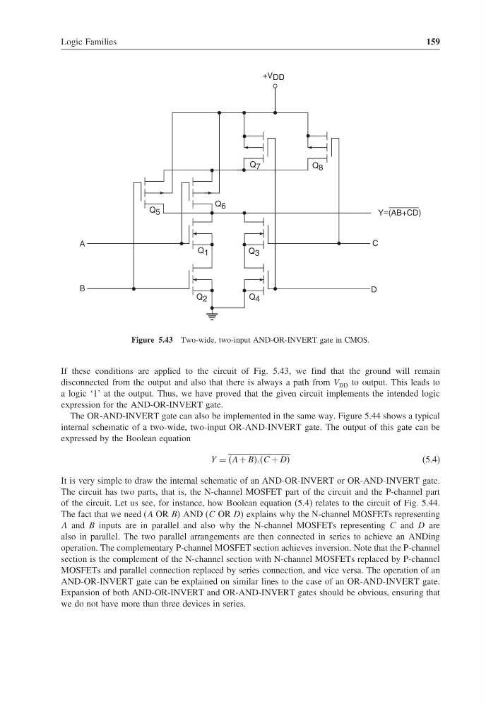
Figure 5.43 Two-wide, two-input AND-OR-INVERT gate in CMOS.
If these conditions are applied to the circuit of Fig. 5.43, we find that the ground will remain
disconnected from the output and also that there is always a path from V DD to output. This leads to
a logic ‘1’ at the output. Thus, we have proved that the given circuit implements the intended logic
expression for the AND-OR-INVERT gate.
The OR-AND-INVERT gate can also be implemented in the same way. Figure 5.44 shows a typical
internal schematic of a two-wide, two-input OR-AND-INVERT gate. The output of this gate can be
expressed by the Boolean equation
Y = A + BBBBC + DD
(5.4)
It is very simple to draw the internal schematic of an AND-OR-INVERT or OR-AND-INVERT gate.
The circuit has two parts, that is, the N-channel MOSFET part of the circuit and the P-channel part
of the circuit. Let us see, for instance, how Boolean equation (5.4) relates to the circuit of Fig. 5.44.
The fact that we need (A OR BB AND (C OR DD explains why the N-channel MOSFETs representing
A and B inputs are in parallel and also why the N-channel MOSFETs representing C and D are
also in parallel. The two parallel arrangements are then connected in series to achieve an ANDing
operation. The complementary P-channel MOSFET section achieves inversion. Note that the P-channel
section is the complement of the N-channel section with N-channel MOSFETs replaced by P-channel
MOSFETs and parallel connection replaced by series connection, and vice versa. The operation of an
AND-OR-INVERT gate can be explained on similar lines to the case of an OR-AND-INVERT gate.
Expansion of both AND-OR-INVERT and OR-AND-INVERT gates should be obvious, ensuring that
we do not have more than three devices in series.
159
Q 5
Q 6
Q 8
Q 7
Q 1
Q 3
Q 2
Q 4
C
D
A
B
+V DD
Y=(AB+CD)
Figure 5.43 Two-wide, two-input AND-OR-INVERT gate in CMOS.
If these conditions are applied to the circuit of Fig. 5.43, we find that the ground will remain
disconnected from the output and also that there is always a path from V DD to output. This leads to
a logic ‘1’ at the output. Thus, we have proved that the given circuit implements the intended logic
expression for the AND-OR-INVERT gate.
The OR-AND-INVERT gate can also be implemented in the same way. Figure 5.44 shows a typical
internal schematic of a two-wide, two-input OR-AND-INVERT gate. The output of this gate can be
expressed by the Boolean equation
Y = A + BBBBC + DD
(5.4)
It is very simple to draw the internal schematic of an AND-OR-INVERT or OR-AND-INVERT gate.
The circuit has two parts, that is, the N-channel MOSFET part of the circuit and the P-channel part
of the circuit. Let us see, for instance, how Boolean equation (5.4) relates to the circuit of Fig. 5.44.
The fact that we need (A OR BB AND (C OR DD explains why the N-channel MOSFETs representing
A and B inputs are in parallel and also why the N-channel MOSFETs representing C and D are
also in parallel. The two parallel arrangements are then connected in series to achieve an ANDing
operation. The complementary P-channel MOSFET section achieves inversion. Note that the P-channel
section is the complement of the N-channel section with N-channel MOSFETs replaced by P-channel
MOSFETs and parallel connection replaced by series connection, and vice versa. The operation of an
AND-OR-INVERT gate can be explained on similar lines to the case of an OR-AND-INVERT gate.
Expansion of both AND-OR-INVERT and OR-AND-INVERT gates should be obvious, ensuring that
we do not have more than three devices in series.