

Logic Families
153
Y=A.B.C
A
B
C
Q 1
V DD
Q 4
Q 5
Q 6
Q 2
Q 3
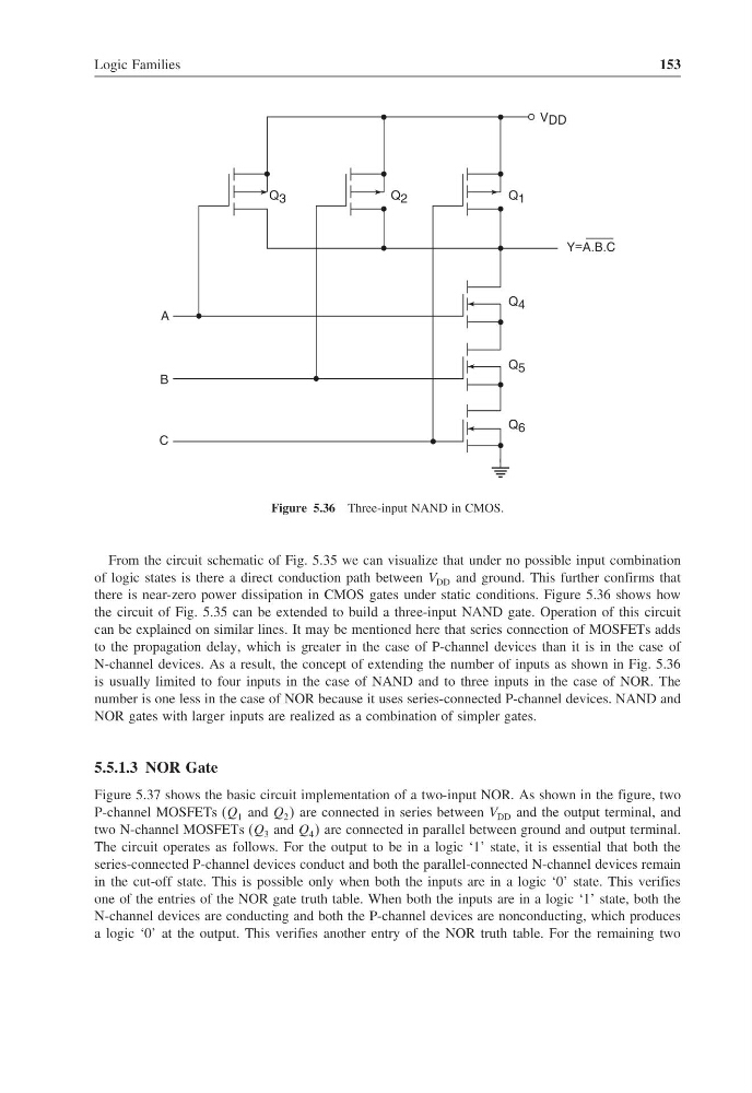
Figure 5.36 Three-input NAND in CMOS.
From the circuit schematic of Fig. 5.35 we can visualize that under no possible input combination
of logic states is there a direct conduction path between V DD and ground. This further confirms that
there is near-zero power dissipation in CMOS gates under static conditions. Figure 5.36 shows how
the circuit of Fig. 5.35 can be extended to build a three-input NAND gate. Operation of this circuit
can be explained on similar lines. It may be mentioned here that series connection of MOSFETs adds
to the propagation delay, which is greater in the case of P-channel devices than it is in the case of
N-channel devices. As a result, the concept of extending the number of inputs as shown in Fig. 5.36
is usually limited to four inputs in the case of NAND and to three inputs in the case of NOR. The
number is one less in the case of NOR because it uses series-connected P-channel devices. NAND and
NOR gates with larger inputs are realized as a combination of simpler gates.
5.5.1.3 NOR Gate
Figure 5.37 shows the basic circuit implementation of a two-input NOR. As shown in the figure, two
P-channel MOSFETs (Q 1 and Q 2 are connected in series between V DD and the output terminal, and
two N-channel MOSFETs (Q 3 and Q 4 are connected in parallel between ground and output terminal.
The circuit operates as follows. For the output to be in a logic ‘1’ state, it is essential that both the
series-connected P-channel devices conduct and both the parallel-connected N-channel devices remain
in the cut-off state. This is possible only when both the inputs are in a logic ‘0’ state. This verifies
one of the entries of the NOR gate truth table. When both the inputs are in a logic ‘1’ state, both the
N-channel devices are conducting and both the P-channel devices are nonconducting, which produces
a logic ‘0’ at the output. This verifies another entry of the NOR truth table. For the remaining two
153
Y=A.B.C
A
B
C
Q 1
V DD
Q 4
Q 5
Q 6
Q 2
Q 3
Figure 5.36 Three-input NAND in CMOS.
From the circuit schematic of Fig. 5.35 we can visualize that under no possible input combination
of logic states is there a direct conduction path between V DD and ground. This further confirms that
there is near-zero power dissipation in CMOS gates under static conditions. Figure 5.36 shows how
the circuit of Fig. 5.35 can be extended to build a three-input NAND gate. Operation of this circuit
can be explained on similar lines. It may be mentioned here that series connection of MOSFETs adds
to the propagation delay, which is greater in the case of P-channel devices than it is in the case of
N-channel devices. As a result, the concept of extending the number of inputs as shown in Fig. 5.36
is usually limited to four inputs in the case of NAND and to three inputs in the case of NOR. The
number is one less in the case of NOR because it uses series-connected P-channel devices. NAND and
NOR gates with larger inputs are realized as a combination of simpler gates.
5.5.1.3 NOR Gate
Figure 5.37 shows the basic circuit implementation of a two-input NOR. As shown in the figure, two
P-channel MOSFETs (Q 1 and Q 2 are connected in series between V DD and the output terminal, and
two N-channel MOSFETs (Q 3 and Q 4 are connected in parallel between ground and output terminal.
The circuit operates as follows. For the output to be in a logic ‘1’ state, it is essential that both the
series-connected P-channel devices conduct and both the parallel-connected N-channel devices remain
in the cut-off state. This is possible only when both the inputs are in a logic ‘0’ state. This verifies
one of the entries of the NOR gate truth table. When both the inputs are in a logic ‘1’ state, both the
N-channel devices are conducting and both the P-channel devices are nonconducting, which produces
a logic ‘0’ at the output. This verifies another entry of the NOR truth table. For the remaining two