

154
Digital Electronics
Y=(A+B)
Q 1
Q 2
V DD
Q 4
Q 3
A
B
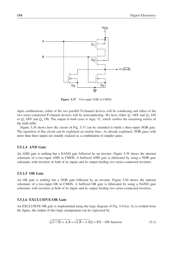
Figure 5.37 Two-input NOR in CMOS.
input combinations, either of the two parallel N-channel devices will be conducting and either of the
two series-connected P-channel devices will be nonconducting. We have either Q 1 OFF and Q 3 ON
or Q 2 OFF and Q 4 ON. The output in both cases is logic ‘0’, which verifies the remaining entries of
the truth table.
Figure 5.38 shows how the circuit of Fig. 5.37 can be extended to build a three-input NOR gate.
The operation of this circuit can be explained on similar lines. As already explained, NOR gates with
more than three inputs are usually realized as a combination of simpler gates.
5.5.1.4 AND Gate
An AND gate is nothing but a NAND gate followed by an inverter. Figure 5.39 shows the internal
schematic of a two-input AND in CMOS. A buffered AND gate is fabricated by using a NOR gate
schematic with inverters at both of its inputs and its output feeding two series-connected inverters.
5.5.1.5 OR Gate
An OR gate is nothing but a NOR gate followed by an inverter. Figure 5.40 shows the internal
schematic of a two-input OR in CMOS. A buffered OR gate is fabricated by using a NAND gate
schematic with inverters at both of its inputs and its output feeding two series-connected inverters.
5.5.1.6 EXCLUSIVE-OR Gate
An EXCLUSIVE-OR gate is implemented using the logic diagram of Fig. 5.41(a). As is evident from
the figure, the output of this logic arrangement can be expressed by
A + BB + AAB = AAB + AABBB = EX − OR function
(5.1)
Digital Electronics
Y=(A+B)
Q 1
Q 2
V DD
Q 4
Q 3
A
B
Figure 5.37 Two-input NOR in CMOS.
input combinations, either of the two parallel N-channel devices will be conducting and either of the
two series-connected P-channel devices will be nonconducting. We have either Q 1 OFF and Q 3 ON
or Q 2 OFF and Q 4 ON. The output in both cases is logic ‘0’, which verifies the remaining entries of
the truth table.
Figure 5.38 shows how the circuit of Fig. 5.37 can be extended to build a three-input NOR gate.
The operation of this circuit can be explained on similar lines. As already explained, NOR gates with
more than three inputs are usually realized as a combination of simpler gates.
5.5.1.4 AND Gate
An AND gate is nothing but a NAND gate followed by an inverter. Figure 5.39 shows the internal
schematic of a two-input AND in CMOS. A buffered AND gate is fabricated by using a NOR gate
schematic with inverters at both of its inputs and its output feeding two series-connected inverters.
5.5.1.5 OR Gate
An OR gate is nothing but a NOR gate followed by an inverter. Figure 5.40 shows the internal
schematic of a two-input OR in CMOS. A buffered OR gate is fabricated by using a NAND gate
schematic with inverters at both of its inputs and its output feeding two series-connected inverters.
5.5.1.6 EXCLUSIVE-OR Gate
An EXCLUSIVE-OR gate is implemented using the logic diagram of Fig. 5.41(a). As is evident from
the figure, the output of this logic arrangement can be expressed by
A + BB + AAB = AAB + AABBB = EX − OR function
(5.1)