

152
Digital Electronics
functions as follows. When the input is in the HIGH state (logic ‘1’), P-channel MOSFET Q 1 is in
the cut-off state while the N-channel MOSFET Q 2 is conducting. The conducting MOSFET provides
a path from ground to output and the output is LOW (logic ‘0’). When the input is in the LOW state
(logic ‘0’), Q 1 is in conduction while Q 2 is in cut-off. The conducting P-channel device provides a path
for V DD to appear at the output, so that the output is in HIGH or logic ‘1’ state. A floating input could
lead to conduction of both MOSFETs and a short-circuit condition. It should therefore be avoided. It
is also evident from Fig. 5.34 that there is no conduction path between V DD and ground in either of
the input conditions, that is, when input is in logic ‘1’ and ‘0’ states. That is why there is practically
zero power dissipation in static conditions. There is only dynamic power dissipation, which occurs
during switching operations as the MOSFET gate capacitance is charged and discharged. The power
dissipated is directly proportional to the switching frequency.
5.5.1.2 NAND Gate
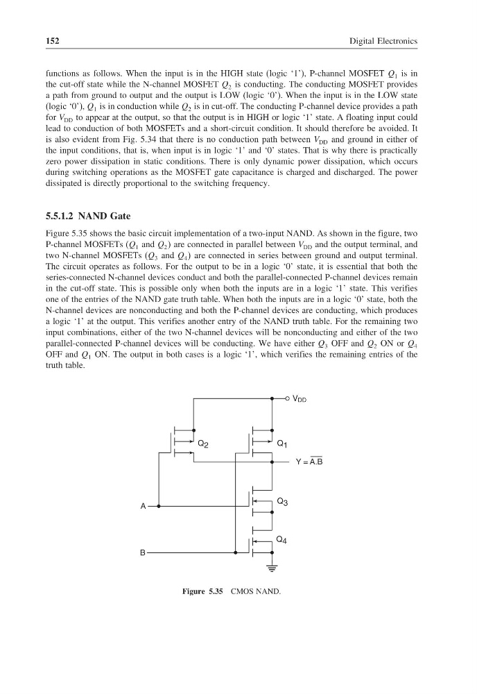
Figure 5.35 shows the basic circuit implementation of a two-input NAND. As shown in the figure, two
P-channel MOSFETs (Q 1 and Q 2 are connected in parallel between V DD and the output terminal, and
two N-channel MOSFETs (Q 3 and Q 4 are connected in series between ground and output terminal.
The circuit operates as follows. For the output to be in a logic ‘0’ state, it is essential that both the
series-connected N-channel devices conduct and both the parallel-connected P-channel devices remain
in the cut-off state. This is possible only when both the inputs are in a logic ‘1’ state. This verifies
one of the entries of the NAND gate truth table. When both the inputs are in a logic ‘0’ state, both the
N-channel devices are nonconducting and both the P-channel devices are conducting, which produces
a logic ‘1’ at the output. This verifies another entry of the NAND truth table. For the remaining two
input combinations, either of the two N-channel devices will be nonconducting and either of the two
parallel-connected P-channel devices will be conducting. We have either Q 3 OFF and Q 2 ON or Q 4
OFF and Q 1 ON. The output in both cases is a logic ‘1’, which verifies the remaining entries of the
truth table.
Y = A.B
V DD
Q 1
Q 2
Q 3
Q 4
A
B
Figure 5.35 CMOS NAND.
Digital Electronics
functions as follows. When the input is in the HIGH state (logic ‘1’), P-channel MOSFET Q 1 is in
the cut-off state while the N-channel MOSFET Q 2 is conducting. The conducting MOSFET provides
a path from ground to output and the output is LOW (logic ‘0’). When the input is in the LOW state
(logic ‘0’), Q 1 is in conduction while Q 2 is in cut-off. The conducting P-channel device provides a path
for V DD to appear at the output, so that the output is in HIGH or logic ‘1’ state. A floating input could
lead to conduction of both MOSFETs and a short-circuit condition. It should therefore be avoided. It
is also evident from Fig. 5.34 that there is no conduction path between V DD and ground in either of
the input conditions, that is, when input is in logic ‘1’ and ‘0’ states. That is why there is practically
zero power dissipation in static conditions. There is only dynamic power dissipation, which occurs
during switching operations as the MOSFET gate capacitance is charged and discharged. The power
dissipated is directly proportional to the switching frequency.
5.5.1.2 NAND Gate
Figure 5.35 shows the basic circuit implementation of a two-input NAND. As shown in the figure, two
P-channel MOSFETs (Q 1 and Q 2 are connected in parallel between V DD and the output terminal, and
two N-channel MOSFETs (Q 3 and Q 4 are connected in series between ground and output terminal.
The circuit operates as follows. For the output to be in a logic ‘0’ state, it is essential that both the
series-connected N-channel devices conduct and both the parallel-connected P-channel devices remain
in the cut-off state. This is possible only when both the inputs are in a logic ‘1’ state. This verifies
one of the entries of the NAND gate truth table. When both the inputs are in a logic ‘0’ state, both the
N-channel devices are nonconducting and both the P-channel devices are conducting, which produces
a logic ‘1’ at the output. This verifies another entry of the NAND truth table. For the remaining two
input combinations, either of the two N-channel devices will be nonconducting and either of the two
parallel-connected P-channel devices will be conducting. We have either Q 3 OFF and Q 2 ON or Q 4
OFF and Q 1 ON. The output in both cases is a logic ‘1’, which verifies the remaining entries of the
truth table.
Y = A.B
V DD
Q 1
Q 2
Q 3
Q 4
A
B
Figure 5.35 CMOS NAND.