

144
Digital Electronics
Driven Gate
Driving Gate
I IH
I IH
I OH
+V CC
+V CC
R 1
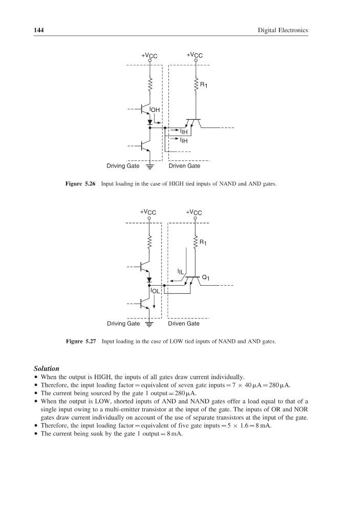
Figure 5.26 Input loading in the case of HIGH tied inputs of NAND and AND gates.
Driven Gate
Driving Gate
I IL
+V CC
+V CC
R 1
Q 1
I OL
Figure 5.27 Input loading in the case of LOW tied inputs of NAND and AND gates.
Solution
• When the output is HIGH, the inputs of all gates draw current individually.
• Therefore, the input loading factor = equivalent of seven gate inputs = 7 × 40 A = 280 A.
• The current being sourced by the gate 1 output = 280 A.
• When the output is LOW, shorted inputs of AND and NAND gates offer a load equal to that of a
single input owing to a multi-emitter transistor at the input of the gate. The inputs of OR and NOR
gates draw current individually on account of the use of separate transistors at the input of the gate.
• Therefore, the input loading factor = equivalent of five gate inputs = 5 × 1.6 = 8 mA.
• The current being sunk by the gate 1 output = 8 mA.
Digital Electronics
Driven Gate
Driving Gate
I IH
I IH
I OH
+V CC
+V CC
R 1
Figure 5.26 Input loading in the case of HIGH tied inputs of NAND and AND gates.
Driven Gate
Driving Gate
I IL
+V CC
+V CC
R 1
Q 1
I OL
Figure 5.27 Input loading in the case of LOW tied inputs of NAND and AND gates.
Solution
• When the output is HIGH, the inputs of all gates draw current individually.
• Therefore, the input loading factor = equivalent of seven gate inputs = 7 × 40 A = 280 A.
• The current being sourced by the gate 1 output = 280 A.
• When the output is LOW, shorted inputs of AND and NAND gates offer a load equal to that of a
single input owing to a multi-emitter transistor at the input of the gate. The inputs of OR and NOR
gates draw current individually on account of the use of separate transistors at the input of the gate.
• Therefore, the input loading factor = equivalent of five gate inputs = 5 × 1.6 = 8 mA.
• The current being sunk by the gate 1 output = 8 mA.