

140
Digital Electronics
features of ALS-TTL and AS-TTL have been discussed at length in the preceding paragraphs. As is
obvious from the internal circuit schematic of the AS-TTL NAND gate, it has some additional circuits
not found in ALS-TTL devices. These are added to enhance the throughput of AS-TTL family devices.
Transistor Q 10 provides a discharge path for the base-collector capacitance of Q 5 . In the absence of
Q 10 , a rising voltage across the output forces current into the base of Q 5 through its base-collector
capacitance, thus causing it to turn on. Transistor Q 10 turns on through D 9 , thus keeping transistor Q 5
in the cut-off state.
5.3.8.1 Characteristic Features
Characteristic features of this family are summarized as follows: V IH = 2 V; V IL = 0.8 V; I IH = 20 A;
I IL = 0.5 mA; V OH = (V CC −2) V; V OL = 0.5 V; I OH = 2 mA; I OL = 20 mA; V CC = 4.5–5.5 V; propagation
delay (for a load resistance of 50 , a load capacitance of 50 pF, V CC = 4.5–5.5 V and an ambient
temperature of minimum to maximum) = 4.5 ns/5 ns (max.) for LOW-to-HIGH and 4 ns/5 ns (max.) for
HIGH-to-LOW output transitions (74AS/54AS); worst-case noise margin = 0.3 V; fan-out = 40; I CCH
(for all four gates) = 3.2 mA; I CCL (for all four gates) = 17.4 mA; operating temperature range = 0–70 °C
(74-series) and −55 to +125 °C (54-series); speed–power product = 13.6 pJ; maximum flip-flop toggle
frequency = 200 MHz.
5.3.9 Fairchild Advanced Schottky TTL (74F/54F)
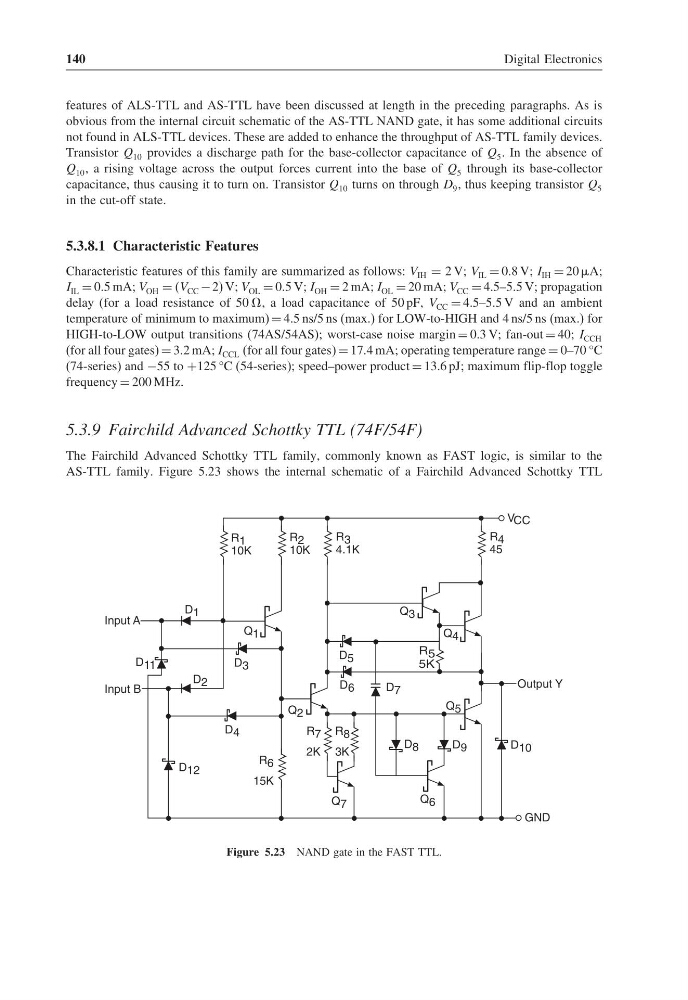
The Fairchild Advanced Schottky TTL family, commonly known as FAST logic, is similar to the
AS-TTL family. Figure 5.23 shows the internal schematic of a Fairchild Advanced Schottky TTL
R 1
10K
R 2
10K
R 3
4.1K
R 4
45
Q 4
Q 3
R 5
5K
D 5
D 6
D 7
Q 5
D 10
GND
Q 6
D 8
D 9
Q 7
R 7
2K
R 8
3K
R 6
15K
D 12
D 4
D 2
D 11
Input B
Input A
D 1
D 3
Q 1
V CC
Output Y
Q 2
Figure 5.23 NAND gate in the FAST TTL.
Digital Electronics
features of ALS-TTL and AS-TTL have been discussed at length in the preceding paragraphs. As is
obvious from the internal circuit schematic of the AS-TTL NAND gate, it has some additional circuits
not found in ALS-TTL devices. These are added to enhance the throughput of AS-TTL family devices.
Transistor Q 10 provides a discharge path for the base-collector capacitance of Q 5 . In the absence of
Q 10 , a rising voltage across the output forces current into the base of Q 5 through its base-collector
capacitance, thus causing it to turn on. Transistor Q 10 turns on through D 9 , thus keeping transistor Q 5
in the cut-off state.
5.3.8.1 Characteristic Features
Characteristic features of this family are summarized as follows: V IH = 2 V; V IL = 0.8 V; I IH = 20 A;
I IL = 0.5 mA; V OH = (V CC −2) V; V OL = 0.5 V; I OH = 2 mA; I OL = 20 mA; V CC = 4.5–5.5 V; propagation
delay (for a load resistance of 50 , a load capacitance of 50 pF, V CC = 4.5–5.5 V and an ambient
temperature of minimum to maximum) = 4.5 ns/5 ns (max.) for LOW-to-HIGH and 4 ns/5 ns (max.) for
HIGH-to-LOW output transitions (74AS/54AS); worst-case noise margin = 0.3 V; fan-out = 40; I CCH
(for all four gates) = 3.2 mA; I CCL (for all four gates) = 17.4 mA; operating temperature range = 0–70 °C
(74-series) and −55 to +125 °C (54-series); speed–power product = 13.6 pJ; maximum flip-flop toggle
frequency = 200 MHz.
5.3.9 Fairchild Advanced Schottky TTL (74F/54F)
The Fairchild Advanced Schottky TTL family, commonly known as FAST logic, is similar to the
AS-TTL family. Figure 5.23 shows the internal schematic of a Fairchild Advanced Schottky TTL
R 1
10K
R 2
10K
R 3
4.1K
R 4
45
Q 4
Q 3
R 5
5K
D 5
D 6
D 7
Q 5
D 10
GND
Q 6
D 8
D 9
Q 7
R 7
2K
R 8
3K
R 6
15K
D 12
D 4
D 2
D 11
Input B
Input A
D 1
D 3
Q 1
V CC
Output Y
Q 2
Figure 5.23 NAND gate in the FAST TTL.