

136
Digital Electronics
5.3.5.1 Characteristic Features
Characteristic features of this family are summarized as follows: V IH = 2 V; V IL = 0.8 V; I IH = 50 A;
I IL = 2 mA; V OH = 2.7 V; V OL = 0.5 V; I OH = 1 mA; I OL = 20 mA; V CC = 4.75–5.25 V (74-series) and
4.5–5.5 V (54-series); propagation delay (for a load resistance of 280 , a load capacitance of 15 pF,
V CC = 5 V and an ambient temperature of 25 °C) = 5 ns (max.) for LOW-to-HIGH and 4.5 ns (max.)
for HIGH-to-LOW output transitions; worst-case noise margin = 0.3 V; fan-out = 10; I CCH (for all
four gates) = 16 mA; I CCL (for all four gates) = 36 mA; operating temperature range = 0–70 °C (74series) and −55 to +125 °C (54-series); speed–power product = 57 pJ; maximum flip-flop toggle
frequency = 125 MHz.
5.3.6 Low-Power Schottky TTL (74LS/54LS)
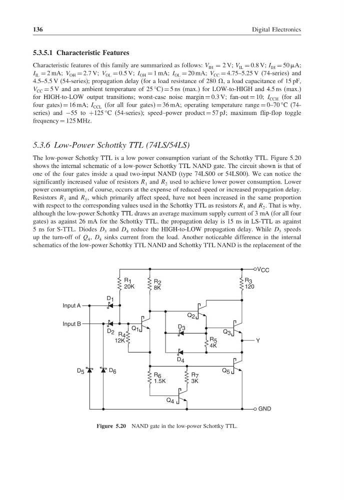
The low-power Schottky TTL is a low power consumption variant of the Schottky TTL. Figure 5.20
shows the internal schematic of a low-power Schottky TTL NAND gate. The circuit shown is that of
one of the four gates inside a quad two-input NAND (type 74LS00 or 54LS00). We can notice the
significantly increased value of resistors R 1 and R 2 used to achieve lower power consumption. Lower
power consumption, of course, occurs at the expense of reduced speed or increased propagation delay.
Resistors R 3 and R 5 , which primarily affect speed, have not been increased in the same proportion
with respect to the corresponding values used in the Schottky TTL as resistors R 1 and R 2 . That is why,
although the low-power Schottky TTL draws an average maximum supply current of 3 mA (for all four
gates) as against 26 mA for the Schottky TTL, the propagation delay is 15 ns in LS-TTL as against
5 ns for S-TTL. Diodes D 3 and D 4 reduce the HIGH-to-LOW propagation delay. While D 3 speeds
up the turn-off of Q 4 , D 4 sinks current from the load. Another noticeable difference in the internal
schematics of the low-power Schottky TTL NAND and Schottky TTL NAND is the replacement of the
V CC
Y
GND
Q 4
R 7
3K
R 5
4K
Q 3
Q 5
R 3
120
R 2
8K
R 1
20K
D 1
D 2
Input A
Input B
R 6
1.5K
Q 2
Q 1
D 3
D 4
12K
R 4
D 6
D 5
Figure 5.20 NAND gate in the low-power Schottky TTL.
Digital Electronics
5.3.5.1 Characteristic Features
Characteristic features of this family are summarized as follows: V IH = 2 V; V IL = 0.8 V; I IH = 50 A;
I IL = 2 mA; V OH = 2.7 V; V OL = 0.5 V; I OH = 1 mA; I OL = 20 mA; V CC = 4.75–5.25 V (74-series) and
4.5–5.5 V (54-series); propagation delay (for a load resistance of 280 , a load capacitance of 15 pF,
V CC = 5 V and an ambient temperature of 25 °C) = 5 ns (max.) for LOW-to-HIGH and 4.5 ns (max.)
for HIGH-to-LOW output transitions; worst-case noise margin = 0.3 V; fan-out = 10; I CCH (for all
four gates) = 16 mA; I CCL (for all four gates) = 36 mA; operating temperature range = 0–70 °C (74series) and −55 to +125 °C (54-series); speed–power product = 57 pJ; maximum flip-flop toggle
frequency = 125 MHz.
5.3.6 Low-Power Schottky TTL (74LS/54LS)
The low-power Schottky TTL is a low power consumption variant of the Schottky TTL. Figure 5.20
shows the internal schematic of a low-power Schottky TTL NAND gate. The circuit shown is that of
one of the four gates inside a quad two-input NAND (type 74LS00 or 54LS00). We can notice the
significantly increased value of resistors R 1 and R 2 used to achieve lower power consumption. Lower
power consumption, of course, occurs at the expense of reduced speed or increased propagation delay.
Resistors R 3 and R 5 , which primarily affect speed, have not been increased in the same proportion
with respect to the corresponding values used in the Schottky TTL as resistors R 1 and R 2 . That is why,
although the low-power Schottky TTL draws an average maximum supply current of 3 mA (for all four
gates) as against 26 mA for the Schottky TTL, the propagation delay is 15 ns in LS-TTL as against
5 ns for S-TTL. Diodes D 3 and D 4 reduce the HIGH-to-LOW propagation delay. While D 3 speeds
up the turn-off of Q 4 , D 4 sinks current from the load. Another noticeable difference in the internal
schematics of the low-power Schottky TTL NAND and Schottky TTL NAND is the replacement of the
V CC
Y
GND
Q 4
R 7
3K
R 5
4K
Q 3
Q 5
R 3
120
R 2
8K
R 1
20K
D 1
D 2
Input A
Input B
R 6
1.5K
Q 2
Q 1
D 3
D 4
12K
R 4
D 6
D 5
Figure 5.20 NAND gate in the low-power Schottky TTL.