

Logic Families
135
5.3.4.1 Characteristic Features
Characteristic features of this family are summarized as follows: V IH = 2 V; V IL = 0.8 V; I IH = 50 A;
I IL = 2 mA; V OH = 2.4 V; V OL = 0.4 V; I OH = 500 A; I OL = 20 mA; V CC = 4.75–5.25 V (74-series)
and 4.5–5.5 V (54-series); propagation delay (for a load resistance of 280 , a load capacitance
of 25 pF, V CC = 5 V and an ambient temperature of 25 °C) = 10 ns (max.) for both LOW-to-HIGH
and HIGH-to-LOW output transitions; worst–case noise margin = 0.4 V; fan-out = 10; I CCH (for
all four gates) = 16.8 mA; I CCL (for all four gates) = 40 mA; operating temperature range = 0–70 °C
(74-series) and −55 to +125 °C (54-series); speed–power product = 132 pJ; maximum flip-flop
frequency = 50 MHz.
5.3.5 Schottky TTL (74S/54S)
The Schottky TTL offers a speed that is about twice that offered by the high-power TTL for the
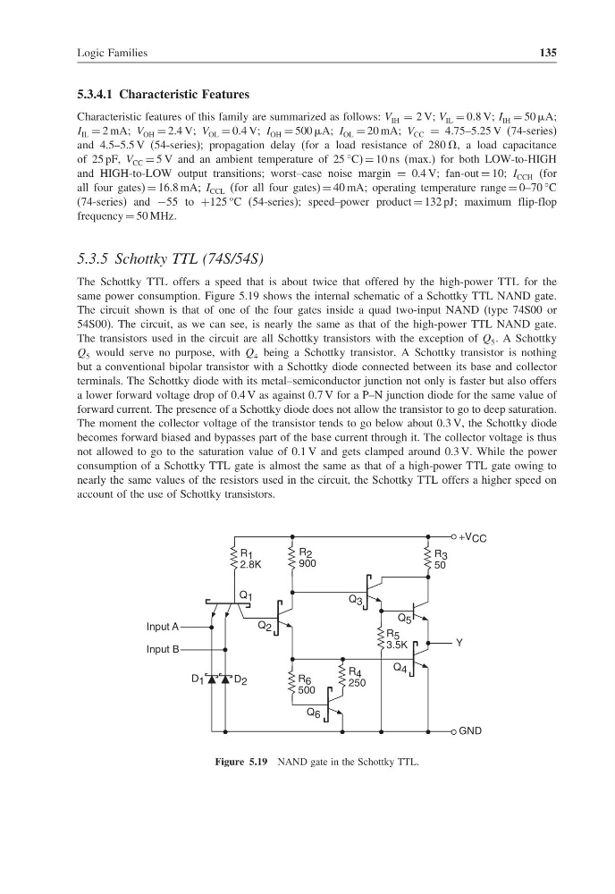
same power consumption. Figure 5.19 shows the internal schematic of a Schottky TTL NAND gate.
The circuit shown is that of one of the four gates inside a quad two-input NAND (type 74S00 or
54S00). The circuit, as we can see, is nearly the same as that of the high-power TTL NAND gate.
The transistors used in the circuit are all Schottky transistors with the exception of Q 5 . A Schottky
Q 5 would serve no purpose, with Q 4 being a Schottky transistor. A Schottky transistor is nothing
but a conventional bipolar transistor with a Schottky diode connected between its base and collector
terminals. The Schottky diode with its metal–semiconductor junction not only is faster but also offers
a lower forward voltage drop of 0.4 V as against 0.7 V for a P–N junction diode for the same value of
forward current. The presence of a Schottky diode does not allow the transistor to go to deep saturation.
The moment the collector voltage of the transistor tends to go below about 0.3 V, the Schottky diode
becomes forward biased and bypasses part of the base current through it. The collector voltage is thus
not allowed to go to the saturation value of 0.1 V and gets clamped around 0.3 V. While the power
consumption of a Schottky TTL gate is almost the same as that of a high-power TTL gate owing to
nearly the same values of the resistors used in the circuit, the Schottky TTL offers a higher speed on
account of the use of Schottky transistors.
Input B
Q 1
Q 2
D 2
R 6
500
Q 4
Q 5
Y
+V CC
R 3
50
R 2
900
R 1
2.8K
Input A
GND
R 5
3.5K
Q 3
D 1
R 4
250
Q 6
Figure 5.19 NAND gate in the Schottky TTL.
135
5.3.4.1 Characteristic Features
Characteristic features of this family are summarized as follows: V IH = 2 V; V IL = 0.8 V; I IH = 50 A;
I IL = 2 mA; V OH = 2.4 V; V OL = 0.4 V; I OH = 500 A; I OL = 20 mA; V CC = 4.75–5.25 V (74-series)
and 4.5–5.5 V (54-series); propagation delay (for a load resistance of 280 , a load capacitance
of 25 pF, V CC = 5 V and an ambient temperature of 25 °C) = 10 ns (max.) for both LOW-to-HIGH
and HIGH-to-LOW output transitions; worst–case noise margin = 0.4 V; fan-out = 10; I CCH (for
all four gates) = 16.8 mA; I CCL (for all four gates) = 40 mA; operating temperature range = 0–70 °C
(74-series) and −55 to +125 °C (54-series); speed–power product = 132 pJ; maximum flip-flop
frequency = 50 MHz.
5.3.5 Schottky TTL (74S/54S)
The Schottky TTL offers a speed that is about twice that offered by the high-power TTL for the
same power consumption. Figure 5.19 shows the internal schematic of a Schottky TTL NAND gate.
The circuit shown is that of one of the four gates inside a quad two-input NAND (type 74S00 or
54S00). The circuit, as we can see, is nearly the same as that of the high-power TTL NAND gate.
The transistors used in the circuit are all Schottky transistors with the exception of Q 5 . A Schottky
Q 5 would serve no purpose, with Q 4 being a Schottky transistor. A Schottky transistor is nothing
but a conventional bipolar transistor with a Schottky diode connected between its base and collector
terminals. The Schottky diode with its metal–semiconductor junction not only is faster but also offers
a lower forward voltage drop of 0.4 V as against 0.7 V for a P–N junction diode for the same value of
forward current. The presence of a Schottky diode does not allow the transistor to go to deep saturation.
The moment the collector voltage of the transistor tends to go below about 0.3 V, the Schottky diode
becomes forward biased and bypasses part of the base current through it. The collector voltage is thus
not allowed to go to the saturation value of 0.1 V and gets clamped around 0.3 V. While the power
consumption of a Schottky TTL gate is almost the same as that of a high-power TTL gate owing to
nearly the same values of the resistors used in the circuit, the Schottky TTL offers a higher speed on
account of the use of Schottky transistors.
Input B
Q 1
Q 2
D 2
R 6
500
Q 4
Q 5
Y
+V CC
R 3
50
R 2
900
R 1
2.8K
Input A
GND
R 5
3.5K
Q 3
D 1
R 4
250
Q 6
Figure 5.19 NAND gate in the Schottky TTL.