

134
Digital Electronics
low-power TTL NAND gate. The circuit shown is that of one of the four gates inside a quad two-input
NAND (type 74L00 or 54L00). The circuit, as we can see, is the same as that of the standard TTL
NAND gate except for an increased resistance value of the different resistors used in the circuit.
Increased resistance values lead to lower power dissipation.
5.3.3.1 Characteristic Features
Characteristic features of this family are summarized as follows: V IH = 2 V; V IL = 0.7 V; I IH = 10 A;
I IL = 0.18 mA; V OH = 2.4 V; V OL = 0.4 V; I OH = 200 A; I OL = 3.6 mA; V CC = 4.75–5.25 V (74-series)
and 4.5–5.5 V (54-series); propagation delay (for a load resistance of 4000 , a load capacitance
of 50 pF, V CC = 5 V and an ambient temperature of 25 °C) = 60 ns (max.) for both LOW-to-HIGH
and HIGH-to-LOW output transitions; worst-case noise margin = 0.3 V; fan-out = 20; I CCH (for all
four gates) = 0.8 mA; I CCL (for all four gates) = 2.04 mA; operating temperature range = 0–70 °C (74series) and −55 to +125 °C (54-series); speed–power product = 33 pJ; maximum flip-flop toggle
frequency = 3 MHz.
5.3.4 High-Power TTL (74H/54H)
The high-power TTL is a high-power, high-speed variant of the standard TTL where improved speed
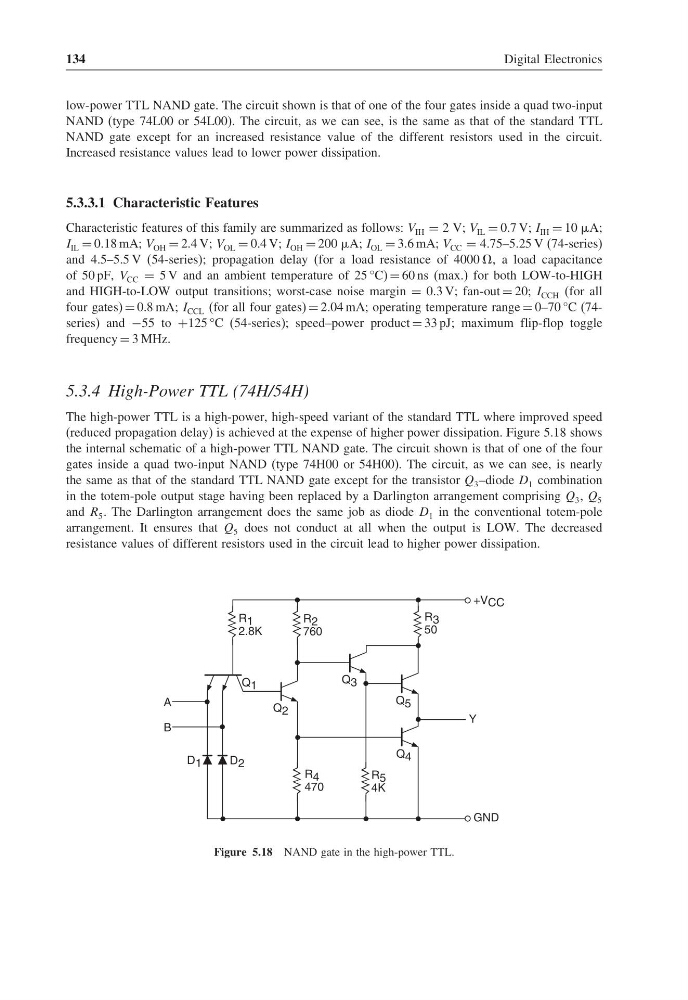
(reduced propagation delay) is achieved at the expense of higher power dissipation. Figure 5.18 shows
the internal schematic of a high-power TTL NAND gate. The circuit shown is that of one of the four
gates inside a quad two-input NAND (type 74H00 or 54H00). The circuit, as we can see, is nearly
the same as that of the standard TTL NAND gate except for the transistor Q 3 –diode D 1 combination
in the totem-pole output stage having been replaced by a Darlington arrangement comprising Q 3 , Q 5
and R 5 . The Darlington arrangement does the same job as diode D 1 in the conventional totem-pole
arrangement. It ensures that Q 5 does not conduct at all when the output is LOW. The decreased
resistance values of different resistors used in the circuit lead to higher power dissipation.
B
Q 1
Q 2
D 2
R 4
470
Q 4
Q 5
Y
+V CC
R 3
50
R 2
760
R 1
2.8K
A
GND
R 5
4K
Q 3
D 1
Figure 5.18 NAND gate in the high-power TTL.
Digital Electronics
low-power TTL NAND gate. The circuit shown is that of one of the four gates inside a quad two-input
NAND (type 74L00 or 54L00). The circuit, as we can see, is the same as that of the standard TTL
NAND gate except for an increased resistance value of the different resistors used in the circuit.
Increased resistance values lead to lower power dissipation.
5.3.3.1 Characteristic Features
Characteristic features of this family are summarized as follows: V IH = 2 V; V IL = 0.7 V; I IH = 10 A;
I IL = 0.18 mA; V OH = 2.4 V; V OL = 0.4 V; I OH = 200 A; I OL = 3.6 mA; V CC = 4.75–5.25 V (74-series)
and 4.5–5.5 V (54-series); propagation delay (for a load resistance of 4000 , a load capacitance
of 50 pF, V CC = 5 V and an ambient temperature of 25 °C) = 60 ns (max.) for both LOW-to-HIGH
and HIGH-to-LOW output transitions; worst-case noise margin = 0.3 V; fan-out = 20; I CCH (for all
four gates) = 0.8 mA; I CCL (for all four gates) = 2.04 mA; operating temperature range = 0–70 °C (74series) and −55 to +125 °C (54-series); speed–power product = 33 pJ; maximum flip-flop toggle
frequency = 3 MHz.
5.3.4 High-Power TTL (74H/54H)
The high-power TTL is a high-power, high-speed variant of the standard TTL where improved speed
(reduced propagation delay) is achieved at the expense of higher power dissipation. Figure 5.18 shows
the internal schematic of a high-power TTL NAND gate. The circuit shown is that of one of the four
gates inside a quad two-input NAND (type 74H00 or 54H00). The circuit, as we can see, is nearly
the same as that of the standard TTL NAND gate except for the transistor Q 3 –diode D 1 combination
in the totem-pole output stage having been replaced by a Darlington arrangement comprising Q 3 , Q 5
and R 5 . The Darlington arrangement does the same job as diode D 1 in the conventional totem-pole
arrangement. It ensures that Q 5 does not conduct at all when the output is LOW. The decreased
resistance values of different resistors used in the circuit lead to higher power dissipation.
B
Q 1
Q 2
D 2
R 4
470
Q 4
Q 5
Y
+V CC
R 3
50
R 2
760
R 1
2.8K
A
GND
R 5
4K
Q 3
D 1
Figure 5.18 NAND gate in the high-power TTL.