

Logic Families
133
Input
ENABLE
Q 1
Q 2
D 1
R 3
Q 4
Q 3
D 2
Y
+V CC
130
R 4
R 2
1.6K
4K
R 1
1K
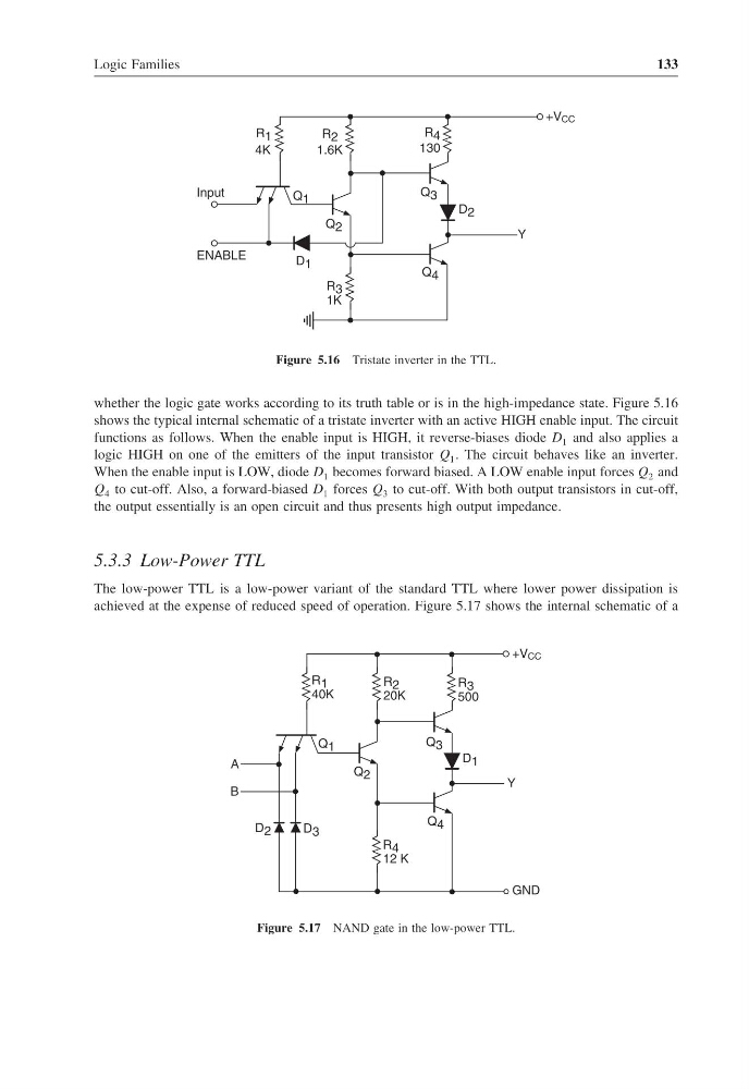
Figure 5.16 Tristate inverter in the TTL.
whether the logic gate works according to its truth table or is in the high-impedance state. Figure 5.16
shows the typical internal schematic of a tristate inverter with an active HIGH enable input. The circuit
functions as follows. When the enable input is HIGH, it reverse-biases diode D 1 and also applies a
logic HIGH on one of the emitters of the input transistor Q 1 . The circuit behaves like an inverter.
When the enable input is LOW, diode D 1 becomes forward biased. A LOW enable input forces Q 2 and
Q 4 to cut-off. Also, a forward-biased D 1 forces Q 3 to cut-off. With both output transistors in cut-off,
the output essentially is an open circuit and thus presents high output impedance.
5.3.3 Low-Power TTL
The low-power TTL is a low-power variant of the standard TTL where lower power dissipation is
achieved at the expense of reduced speed of operation. Figure 5.17 shows the internal schematic of a
B
Q 1
Q 2
D 2
R 4
12 K
Q 4
Q 3
D 1
Y
+V CC
R 3
500
R 2
20K
R 1
40K
A
D 3
GND
Figure 5.17 NAND gate in the low-power TTL.
133
Input
ENABLE
Q 1
Q 2
D 1
R 3
Q 4
Q 3
D 2
Y
+V CC
130
R 4
R 2
1.6K
4K
R 1
1K
Figure 5.16 Tristate inverter in the TTL.
whether the logic gate works according to its truth table or is in the high-impedance state. Figure 5.16
shows the typical internal schematic of a tristate inverter with an active HIGH enable input. The circuit
functions as follows. When the enable input is HIGH, it reverse-biases diode D 1 and also applies a
logic HIGH on one of the emitters of the input transistor Q 1 . The circuit behaves like an inverter.
When the enable input is LOW, diode D 1 becomes forward biased. A LOW enable input forces Q 2 and
Q 4 to cut-off. Also, a forward-biased D 1 forces Q 3 to cut-off. With both output transistors in cut-off,
the output essentially is an open circuit and thus presents high output impedance.
5.3.3 Low-Power TTL
The low-power TTL is a low-power variant of the standard TTL where lower power dissipation is
achieved at the expense of reduced speed of operation. Figure 5.17 shows the internal schematic of a
B
Q 1
Q 2
D 2
R 4
12 K
Q 4
Q 3
D 1
Y
+V CC
R 3
500
R 2
20K
R 1
40K
A
D 3
GND
Figure 5.17 NAND gate in the low-power TTL.