

132
Digital Electronics
Input A
Q 2
4K
Q 3
Output
Y
1.6K
Q 1
V CC
1K
GND
Input B
D 1
D 2
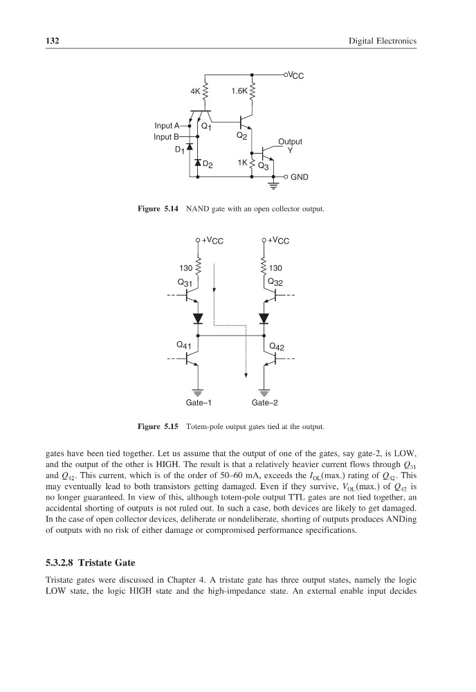
Figure 5.14 NAND gate with an open collector output.
Q 31
Q 41
+V CC
Gate–1
Q 32
130
Q 42
+V CC
Gate–2
130
Figure 5.15 Totem-pole output gates tied at the output.
gates have been tied together. Let us assume that the output of one of the gates, say gate-2, is LOW,
and the output of the other is HIGH. The result is that a relatively heavier current flows through Q 31
and Q 42 . This current, which is of the order of 50–60 mA, exceeds the I OL (max.) rating of Q 42 . This
may eventually lead to both transistors getting damaged. Even if they survive, V OL (max.) of Q 42 is
no longer guaranteed. In view of this, although totem-pole output TTL gates are not tied together, an
accidental shorting of outputs is not ruled out. In such a case, both devices are likely to get damaged.
In the case of open collector devices, deliberate or nondeliberate, shorting of outputs produces ANDing
of outputs with no risk of either damage or compromised performance specifications.
5.3.2.8 Tristate Gate
Tristate gates were discussed in Chapter 4. A tristate gate has three output states, namely the logic
LOW state, the logic HIGH state and the high-impedance state. An external enable input decides
Digital Electronics
Input A
Q 2
4K
Q 3
Output
Y
1.6K
Q 1
V CC
1K
GND
Input B
D 1
D 2
Figure 5.14 NAND gate with an open collector output.
Q 31
Q 41
+V CC
Gate–1
Q 32
130
Q 42
+V CC
Gate–2
130
Figure 5.15 Totem-pole output gates tied at the output.
gates have been tied together. Let us assume that the output of one of the gates, say gate-2, is LOW,
and the output of the other is HIGH. The result is that a relatively heavier current flows through Q 31
and Q 42 . This current, which is of the order of 50–60 mA, exceeds the I OL (max.) rating of Q 42 . This
may eventually lead to both transistors getting damaged. Even if they survive, V OL (max.) of Q 42 is
no longer guaranteed. In view of this, although totem-pole output TTL gates are not tied together, an
accidental shorting of outputs is not ruled out. In such a case, both devices are likely to get damaged.
In the case of open collector devices, deliberate or nondeliberate, shorting of outputs produces ANDing
of outputs with no risk of either damage or compromised performance specifications.
5.3.2.8 Tristate Gate
Tristate gates were discussed in Chapter 4. A tristate gate has three output states, namely the logic
LOW state, the logic HIGH state and the high-impedance state. An external enable input decides