

Logic Families
131
5.3.2.6 AND-OR-INVERT Gate
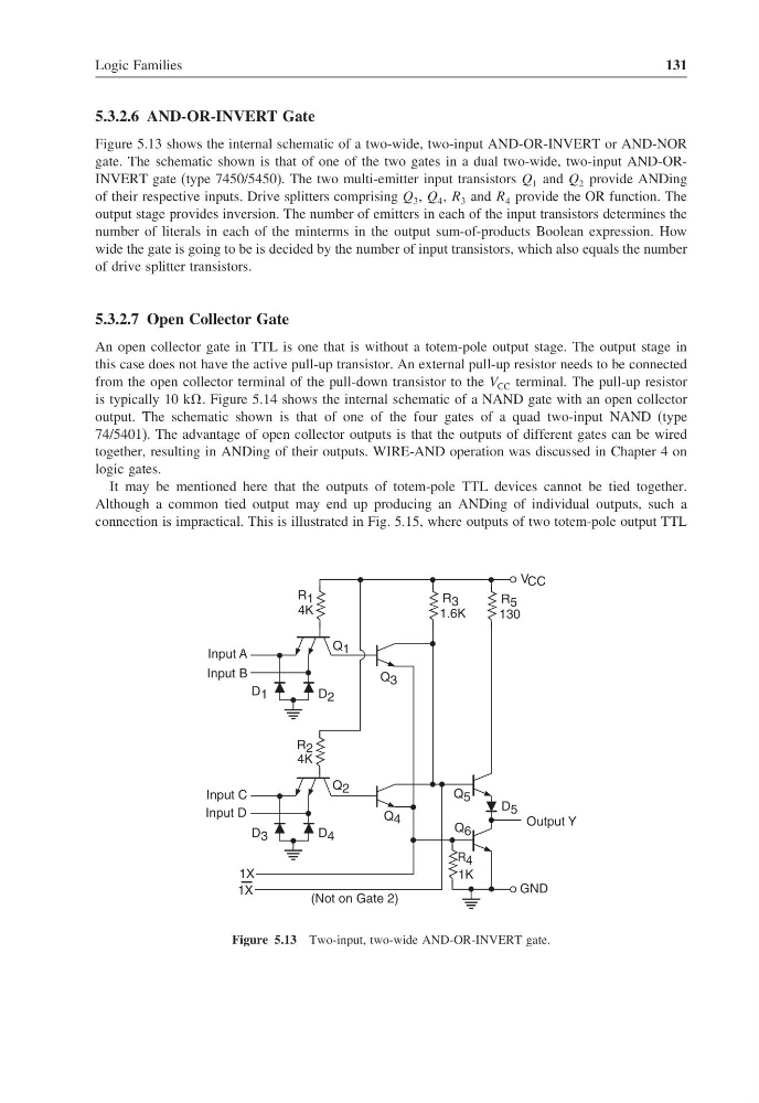
Figure 5.13 shows the internal schematic of a two-wide, two-input AND-OR-INVERT or AND-NOR
gate. The schematic shown is that of one of the two gates in a dual two-wide, two-input AND-ORINVERT gate (type 7450/5450). The two multi-emitter input transistors Q 1 and Q 2 provide ANDing
of their respective inputs. Drive splitters comprising Q 3 , Q 4 , R 3 and R 4 provide the OR function. The
output stage provides inversion. The number of emitters in each of the input transistors determines the
number of literals in each of the minterms in the output sum-of-products Boolean expression. How
wide the gate is going to be is decided by the number of input transistors, which also equals the number
of drive splitter transistors.
5.3.2.7 Open Collector Gate
An open collector gate in TTL is one that is without a totem-pole output stage. The output stage in
this case does not have the active pull-up transistor. An external pull-up resistor needs to be connected
from the open collector terminal of the pull-down transistor to the V CC terminal. The pull-up resistor
is typically 10 k. Figure 5.14 shows the internal schematic of a NAND gate with an open collector
output. The schematic shown is that of one of the four gates of a quad two-input NAND (type
74/5401). The advantage of open collector outputs is that the outputs of different gates can be wired
together, resulting in ANDing of their outputs. WIRE-AND operation was discussed in Chapter 4 on
logic gates.
It may be mentioned here that the outputs of totem-pole TTL devices cannot be tied together.
Although a common tied output may end up producing an ANDing of individual outputs, such a
connection is impractical. This is illustrated in Fig. 5.15, where outputs of two totem-pole output TTL
Input A
1X
(Not on Gate 2)
1X
Q 2
D 4
Q 3
R 3
130
1.6K
4K
R 1
Q 1
D 2
Q 5
D 5
Q 6
R 4
1K
GND
4K
R 2
Q 4
V CC
D 1
D 3
Output Y
Input B
Input C
Input D
R 5
Figure 5.13 Two-input, two-wide AND-OR-INVERT gate.
131
5.3.2.6 AND-OR-INVERT Gate
Figure 5.13 shows the internal schematic of a two-wide, two-input AND-OR-INVERT or AND-NOR
gate. The schematic shown is that of one of the two gates in a dual two-wide, two-input AND-ORINVERT gate (type 7450/5450). The two multi-emitter input transistors Q 1 and Q 2 provide ANDing
of their respective inputs. Drive splitters comprising Q 3 , Q 4 , R 3 and R 4 provide the OR function. The
output stage provides inversion. The number of emitters in each of the input transistors determines the
number of literals in each of the minterms in the output sum-of-products Boolean expression. How
wide the gate is going to be is decided by the number of input transistors, which also equals the number
of drive splitter transistors.
5.3.2.7 Open Collector Gate
An open collector gate in TTL is one that is without a totem-pole output stage. The output stage in
this case does not have the active pull-up transistor. An external pull-up resistor needs to be connected
from the open collector terminal of the pull-down transistor to the V CC terminal. The pull-up resistor
is typically 10 k. Figure 5.14 shows the internal schematic of a NAND gate with an open collector
output. The schematic shown is that of one of the four gates of a quad two-input NAND (type
74/5401). The advantage of open collector outputs is that the outputs of different gates can be wired
together, resulting in ANDing of their outputs. WIRE-AND operation was discussed in Chapter 4 on
logic gates.
It may be mentioned here that the outputs of totem-pole TTL devices cannot be tied together.
Although a common tied output may end up producing an ANDing of individual outputs, such a
connection is impractical. This is illustrated in Fig. 5.15, where outputs of two totem-pole output TTL
Input A
1X
(Not on Gate 2)
1X
Q 2
D 4
Q 3
R 3
130
1.6K
4K
R 1
Q 1
D 2
Q 5
D 5
Q 6
R 4
1K
GND
4K
R 2
Q 4
V CC
D 1
D 3
Output Y
Input B
Input C
Input D
R 5
Figure 5.13 Two-input, two-wide AND-OR-INVERT gate.