

130
Digital Electronics
be in cut-off. This is possible only when both Q 1 and Q 2 are in saturation. That is, both inputs are in
the logic LOW state. This verifies one of the entries of the truth table of the OR gate. Let us now see
what happens when either of the two inputs is driven to the HIGH state. This drives either of the two
transistors Q 3 and Q 4 to saturation, which forces Q 5 to saturation and Q 6 to cut-off. This drives Q 7 to
conduction and Q 8 to cut-off, producing a logic HIGH output.
5.3.2.5 EXCLUSIVE-OR Gate
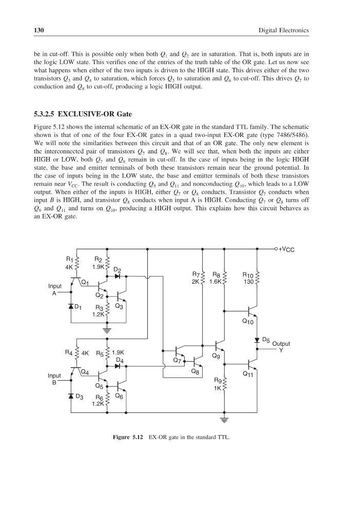
Figure 5.12 shows the internal schematic of an EX-OR gate in the standard TTL family. The schematic
shown is that of one of the four EX-OR gates in a quad two-input EX-OR gate (type 7486/5486).
We will note the similarities between this circuit and that of an OR gate. The only new element is
the interconnected pair of transistors Q 7 and Q 8 . We will see that, when both the inputs are either
HIGH or LOW, both Q 7 and Q 8 remain in cut-off. In the case of inputs being in the logic HIGH
state, the base and emitter terminals of both these transistors remain near the ground potential. In
the case of inputs being in the LOW state, the base and emitter terminals of both these transistors
remain near V CC . The result is conducting Q 9 and Q 11 and nonconducting Q 10 , which leads to a LOW
output. When either of the inputs is HIGH, either Q 7 or Q 8 conducts. Transistor Q 7 conducts when
input B is HIGH, and transistor Q 8 conducts when input A is HIGH. Conducting Q 7 or Q 8 turns off
Q 9 and Q 11 and turns on Q 10 , producing a HIGH output. This explains how this circuit behaves as
an EX-OR gate.
Q 10
R 10
D 5
Q 11
+V CC
Q 9
R 8
R 7
Q 7
Q 8
Q 6
R 6
D 3
Q 4
Q 5
D 4
4K
1.9K
1.2K
Q 1
D 1
A
B
R 4
4K R 5 1.9K
Q 3
Q 2
R 3
R 2
1.6K
130
2K
1K
R 9
1.2K
D 2
Input
Input
R 1
Output
Y
Figure 5.12 EX-OR gate in the standard TTL.
Digital Electronics
be in cut-off. This is possible only when both Q 1 and Q 2 are in saturation. That is, both inputs are in
the logic LOW state. This verifies one of the entries of the truth table of the OR gate. Let us now see
what happens when either of the two inputs is driven to the HIGH state. This drives either of the two
transistors Q 3 and Q 4 to saturation, which forces Q 5 to saturation and Q 6 to cut-off. This drives Q 7 to
conduction and Q 8 to cut-off, producing a logic HIGH output.
5.3.2.5 EXCLUSIVE-OR Gate
Figure 5.12 shows the internal schematic of an EX-OR gate in the standard TTL family. The schematic
shown is that of one of the four EX-OR gates in a quad two-input EX-OR gate (type 7486/5486).
We will note the similarities between this circuit and that of an OR gate. The only new element is
the interconnected pair of transistors Q 7 and Q 8 . We will see that, when both the inputs are either
HIGH or LOW, both Q 7 and Q 8 remain in cut-off. In the case of inputs being in the logic HIGH
state, the base and emitter terminals of both these transistors remain near the ground potential. In
the case of inputs being in the LOW state, the base and emitter terminals of both these transistors
remain near V CC . The result is conducting Q 9 and Q 11 and nonconducting Q 10 , which leads to a LOW
output. When either of the inputs is HIGH, either Q 7 or Q 8 conducts. Transistor Q 7 conducts when
input B is HIGH, and transistor Q 8 conducts when input A is HIGH. Conducting Q 7 or Q 8 turns off
Q 9 and Q 11 and turns on Q 10 , producing a HIGH output. This explains how this circuit behaves as
an EX-OR gate.
Q 10
R 10
D 5
Q 11
+V CC
Q 9
R 8
R 7
Q 7
Q 8
Q 6
R 6
D 3
Q 4
Q 5
D 4
4K
1.9K
1.2K
Q 1
D 1
A
B
R 4
4K R 5 1.9K
Q 3
Q 2
R 3
R 2
1.6K
130
2K
1K
R 9
1.2K
D 2
Input
Input
R 1
Output
Y
Figure 5.12 EX-OR gate in the standard TTL.