

Logic Families
129
V CC
Q 6
Q 5
Q 4
Q 3
Q 2
Q 1
Input A
4K
2K
1.6K
130
Output
Y
GND
800K
1K
Input B
D 1
D 2
D 3
D 4
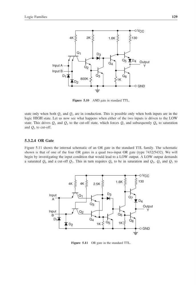
Figure 5.10 AND gate in standard TTL.
state only when both Q 2 and Q 3 are in conduction. This is possible only when both inputs are in the
logic HIGH state. Let us now see what happens when either of the two inputs is driven to the LOW
state. This drives Q 2 and Q 3 to the cut-off state, which forces Q 4 and subsequently Q 6 to saturation
and Q 5 to cut-off.
5.3.2.4 OR Gate
Figure 5.11 shows the internal schematic of an OR gate in the standard TTL family. The schematic
shown is that of one of the four OR gates in a quad two-input OR gate (type 7432/5432). We will
begin by investigating the input condition that would lead to a LOW output. A LOW output demands
a saturated Q 8 and a cut-off Q 7 . This in turn requires Q 6 to be in saturation and Q 5 , Q 4 and Q 3 to
Q 8
Q 7
Q 3
Q 4
Q 2
Q 1
A
B
Input
4K
4K
2.5K
1.6K
130
V CC
GND
Output
Y
1K
Q 5
1K
Q 6
Input
D 1
D 2
D 3
D 4
Figure 5.11 OR gate in the standard TTL.
129
V CC
Q 6
Q 5
Q 4
Q 3
Q 2
Q 1
Input A
4K
2K
1.6K
130
Output
Y
GND
800K
1K
Input B
D 1
D 2
D 3
D 4
Figure 5.10 AND gate in standard TTL.
state only when both Q 2 and Q 3 are in conduction. This is possible only when both inputs are in the
logic HIGH state. Let us now see what happens when either of the two inputs is driven to the LOW
state. This drives Q 2 and Q 3 to the cut-off state, which forces Q 4 and subsequently Q 6 to saturation
and Q 5 to cut-off.
5.3.2.4 OR Gate
Figure 5.11 shows the internal schematic of an OR gate in the standard TTL family. The schematic
shown is that of one of the four OR gates in a quad two-input OR gate (type 7432/5432). We will
begin by investigating the input condition that would lead to a LOW output. A LOW output demands
a saturated Q 8 and a cut-off Q 7 . This in turn requires Q 6 to be in saturation and Q 5 , Q 4 and Q 3 to
Q 8
Q 7
Q 3
Q 4
Q 2
Q 1
A
B
Input
4K
4K
2.5K
1.6K
130
V CC
GND
Output
Y
1K
Q 5
1K
Q 6
Input
D 1
D 2
D 3
D 4
Figure 5.11 OR gate in the standard TTL.