

128
Digital Electronics
4K
130
1.6K
V CC
GND
Output Y
Q 3
Q 2
Q 1
1K
Q 4
Input
A
D 1
D 2
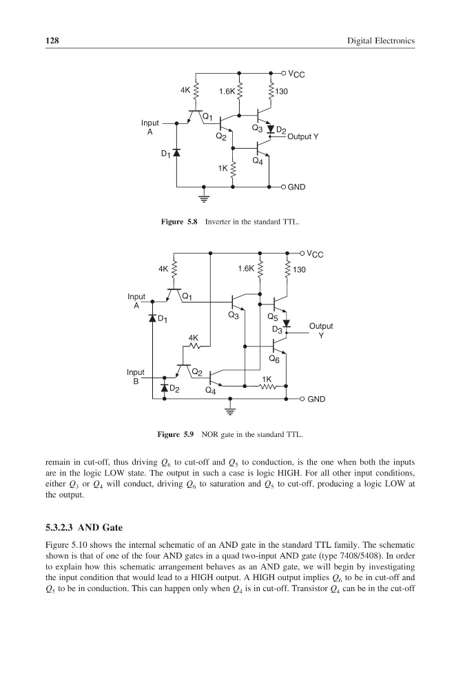
Figure 5.8 Inverter in the standard TTL.
B
A
Input
4K
1.6K
130
V CC
Output
Y
1K
Q 2
Q 4
Q 6
Q 5
Q 1
Q 3
GND
4K
Input
D 1
D 2
D 3
Figure 5.9 NOR gate in the standard TTL.
remain in cut-off, thus driving Q 6 to cut-off and Q 5 to conduction, is the one when both the inputs
are in the logic LOW state. The output in such a case is logic HIGH. For all other input conditions,
either Q 3 or Q 4 will conduct, driving Q 6 to saturation and Q 5 to cut-off, producing a logic LOW at
the output.
5.3.2.3 AND Gate
Figure 5.10 shows the internal schematic of an AND gate in the standard TTL family. The schematic
shown is that of one of the four AND gates in a quad two-input AND gate (type 7408/5408). In order
to explain how this schematic arrangement behaves as an AND gate, we will begin by investigating
the input condition that would lead to a HIGH output. A HIGH output implies Q 6 to be in cut-off and
Q 5 to be in conduction. This can happen only when Q 4 is in cut-off. Transistor Q 4 can be in the cut-off
Digital Electronics
4K
130
1.6K
V CC
GND
Output Y
Q 3
Q 2
Q 1
1K
Q 4
Input
A
D 1
D 2
Figure 5.8 Inverter in the standard TTL.
B
A
Input
4K
1.6K
130
V CC
Output
Y
1K
Q 2
Q 4
Q 6
Q 5
Q 1
Q 3
GND
4K
Input
D 1
D 2
D 3
Figure 5.9 NOR gate in the standard TTL.
remain in cut-off, thus driving Q 6 to cut-off and Q 5 to conduction, is the one when both the inputs
are in the logic LOW state. The output in such a case is logic HIGH. For all other input conditions,
either Q 3 or Q 4 will conduct, driving Q 6 to saturation and Q 5 to cut-off, producing a logic LOW at
the output.
5.3.2.3 AND Gate
Figure 5.10 shows the internal schematic of an AND gate in the standard TTL family. The schematic
shown is that of one of the four AND gates in a quad two-input AND gate (type 7408/5408). In order
to explain how this schematic arrangement behaves as an AND gate, we will begin by investigating
the input condition that would lead to a HIGH output. A HIGH output implies Q 6 to be in cut-off and
Q 5 to be in conduction. This can happen only when Q 4 is in cut-off. Transistor Q 4 can be in the cut-off