

Logic Families
123
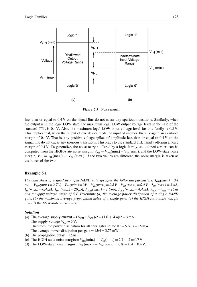
Figure 5.5 Noise margin.
less than or equal to 0.4 V on the signal line do not cause any spurious transitions. Similarly, when
the output is in the logic LOW state, the maximum legal LOW output voltage level in the case of the
standard TTL is 0.4 V. Also, the maximum legal LOW input voltage level for this family is 0.8 V.
This implies that, when the output of one device feeds the input of another, there is again an available
margin of 0.4 V. That is, any positive voltage spikes of amplitude less than or equal to 0.4 V on the
signal line do not cause any spurious transitions. This leads to the standard TTL family offering a noise
margin of 0.4 V. To generalize, the noise margin offered by a logic family, as outlined earlier, can be
computed from the HIGH-state noise margin, V NH = V OH (min.) − V IH (min.), and the LOW-state noise
margin, V NL = V IL (max.) − V OL (max.). If the two values are different, the noise margin is taken as
the lower of the two.
Example 5.1
The data sheet of a quad two-input NAND gate specifies the following parameters: I OH (max.) = 0.4
mA, V OH (min.) = 2.7 V, V IH (min.) = 2V, V IL (max.) = 0.8 V, V OL (max.) = 0.4 V, I OL (max.) = 8 mA,
I IL (max.) = 0.4 mA, I IH (max.) = 20 A, I CCH (max.) = 1.6 mA, I CCL (max.) = 4.4 mA, t pLH = t pHL = 15 ns
and a supply voltage range of 5 V. Determine (a) the average power dissipation of a single NAND
gate, (b) the maximum average propagation delay of a single gate, (c) the HIGH-state noise margin
and (d) the LOW-state noise margin
Solution
(a) The average supply current = (I CCH + I CCL /2 = (1.6 + 4.4)/2 = 3 mA.
The supply voltage V CC = 5 V.
Therefore, the power dissipation for all four gates in the IC = 5 × 3 = 15 mW.
The average power dissipation per gate = 15/4 = 3.75 mW.
(b) The propagation delay = 15 ns.
(c) The HIGH-state noise margin = V OH (min.) − V IH (min.) = 2.7 − 2 = 0.7 V.
(d) The LOW-state noise margin = V IL (max.) − V OL (max.) = 0.8 − 0.4 = 0.4 V.
123
Figure 5.5 Noise margin.
less than or equal to 0.4 V on the signal line do not cause any spurious transitions. Similarly, when
the output is in the logic LOW state, the maximum legal LOW output voltage level in the case of the
standard TTL is 0.4 V. Also, the maximum legal LOW input voltage level for this family is 0.8 V.
This implies that, when the output of one device feeds the input of another, there is again an available
margin of 0.4 V. That is, any positive voltage spikes of amplitude less than or equal to 0.4 V on the
signal line do not cause any spurious transitions. This leads to the standard TTL family offering a noise
margin of 0.4 V. To generalize, the noise margin offered by a logic family, as outlined earlier, can be
computed from the HIGH-state noise margin, V NH = V OH (min.) − V IH (min.), and the LOW-state noise
margin, V NL = V IL (max.) − V OL (max.). If the two values are different, the noise margin is taken as
the lower of the two.
Example 5.1
The data sheet of a quad two-input NAND gate specifies the following parameters: I OH (max.) = 0.4
mA, V OH (min.) = 2.7 V, V IH (min.) = 2V, V IL (max.) = 0.8 V, V OL (max.) = 0.4 V, I OL (max.) = 8 mA,
I IL (max.) = 0.4 mA, I IH (max.) = 20 A, I CCH (max.) = 1.6 mA, I CCL (max.) = 4.4 mA, t pLH = t pHL = 15 ns
and a supply voltage range of 5 V. Determine (a) the average power dissipation of a single NAND
gate, (b) the maximum average propagation delay of a single gate, (c) the HIGH-state noise margin
and (d) the LOW-state noise margin
Solution
(a) The average supply current = (I CCH + I CCL /2 = (1.6 + 4.4)/2 = 3 mA.
The supply voltage V CC = 5 V.
Therefore, the power dissipation for all four gates in the IC = 5 × 3 = 15 mW.
The average power dissipation per gate = 15/4 = 3.75 mW.
(b) The propagation delay = 15 ns.
(c) The HIGH-state noise margin = V OH (min.) − V IH (min.) = 2.7 − 2 = 0.7 V.
(d) The LOW-state noise margin = V IL (max.) − V OL (max.) = 0.8 − 0.4 = 0.4 V.