

Logic Gates and Related Devices
111
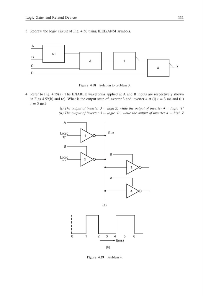
3. Redraw the logic circuit of Fig. 4.56 using IEEE/ANSI symbols.
>1
A
B
C
D
&
1
&
Y
Figure 4.58 Solution to problem 3.
4. Refer to Fig. 4.59(a). The ENABLE waveforms applied at A and B inputs are respectively shown
in Figs 4.59(b) and (c). What is the output state of inverter 3 and inverter 4 at (i) t = 3 ms and (ii)
t = 5 ms?
(i) The output of inverter 3 = high Z, while the output of inverter 4 = logic ‘1’
(ii) The output of inverter 3 = logic ‘0’, while the output of inverter 4 = high Z
Figure 4.59 Problem 4.
111
3. Redraw the logic circuit of Fig. 4.56 using IEEE/ANSI symbols.
>1
A
B
C
D
&
1
&
Y
Figure 4.58 Solution to problem 3.
4. Refer to Fig. 4.59(a). The ENABLE waveforms applied at A and B inputs are respectively shown
in Figs 4.59(b) and (c). What is the output state of inverter 3 and inverter 4 at (i) t = 3 ms and (ii)
t = 5 ms?
(i) The output of inverter 3 = high Z, while the output of inverter 4 = logic ‘1’
(ii) The output of inverter 3 = logic ‘0’, while the output of inverter 4 = high Z
Figure 4.59 Problem 4.