

110
Digital Electronics
(c) a three-input NAND with an open collector output;
(d) a four-input INHIBIT gate.
7. Define the fan-out specification of a logic gate. Which parameters would you need to know from
the data sheet of a logic gate to determine for yourself the fan-out in case it is not mentioned in the
data sheet? Explain the procedure for determining the fan-out specification from those parameters.
What are the consequences of exceeding the fan-out specification?
8. What is the main significance of IEEE/ANSI symbols when compared with the conventional ones?
Draw the ANSI symbols for four-input OR, two-input AND, two-input EX-OR and two-input
NAND gates.
Problems
1. What is the only input combination that:
(a) Will produce a logic ‘1’ at the output of an eight-input AND gate?
(b) Will produce a logic ‘0’ at the output of a four-input NAND gate?
(c) Will produce a logic ‘1’ at the output of an eight-input NOR gate?
(d) Will produce a logic ‘0’ at the output of a four-input OR gate?
(a) 11111111; (b) 1111; (c) 00000000; (d) 0000
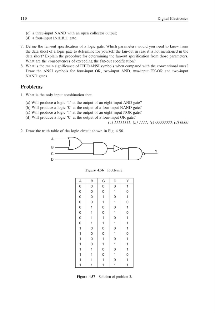
2. Draw the truth table of the logic circuit shown in Fig. 4.56.
Y
A
B
C
D
Figure 4.56 Problem 2.
A
0
0
0
0
0
0
0
0
1
1
1
1
1
1
1
1
B
0
0
0
0
1
1
1
1
0
0
0
0
1
1
1
1
C
0
0
1
1
0
0
1
1
0
0
1
1
0
0
1
1
D
0
1
0
1
0
1
0
1
0
1
0
1
0
1
0
1
Y
1
0
1
0
1
0
1
1
1
0
1
1
1
0
1
1
Figure 4.57 Solution of problem 2.
Digital Electronics
(c) a three-input NAND with an open collector output;
(d) a four-input INHIBIT gate.
7. Define the fan-out specification of a logic gate. Which parameters would you need to know from
the data sheet of a logic gate to determine for yourself the fan-out in case it is not mentioned in the
data sheet? Explain the procedure for determining the fan-out specification from those parameters.
What are the consequences of exceeding the fan-out specification?
8. What is the main significance of IEEE/ANSI symbols when compared with the conventional ones?
Draw the ANSI symbols for four-input OR, two-input AND, two-input EX-OR and two-input
NAND gates.
Problems
1. What is the only input combination that:
(a) Will produce a logic ‘1’ at the output of an eight-input AND gate?
(b) Will produce a logic ‘0’ at the output of a four-input NAND gate?
(c) Will produce a logic ‘1’ at the output of an eight-input NOR gate?
(d) Will produce a logic ‘0’ at the output of a four-input OR gate?
(a) 11111111; (b) 1111; (c) 00000000; (d) 0000
2. Draw the truth table of the logic circuit shown in Fig. 4.56.
Y
A
B
C
D
Figure 4.56 Problem 2.
A
0
0
0
0
0
0
0
0
1
1
1
1
1
1
1
1
B
0
0
0
0
1
1
1
1
0
0
0
0
1
1
1
1
C
0
0
1
1
0
0
1
1
0
0
1
1
0
0
1
1
D
0
1
0
1
0
1
0
1
0
1
0
1
0
1
0
1
Y
1
0
1
0
1
0
1
1
1
0
1
1
1
0
1
1
Figure 4.57 Solution of problem 2.