

90
Digital Electronics
A
B
C
D
E
F
G
(AB+CD+EF+GH)
H
Figure 4.31 Four-wide, two-input AND-OR-INVERT gate.
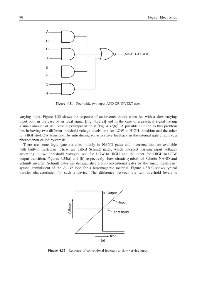
varying input. Figure 4.32 shows the response of an inverter circuit when fed with a slow varying
input both in the case of an ideal signal [Fig. 4.32(a)] and in the case of a practical signal having
a small amount of AC noise superimposed on it [Fig. 4.32(b)]. A possible solution to this problem
lies in having two different threshold voltage levels, one for LOW-to-HIGH transition and the other
for HIGH-to-LOW transition, by introducing some positive feedback in the internal gate circuitry, a
phenomenon called hysteresis.
There are some logic gate varieties, mainly in NAND gates and inverters, that are available
with built-in hysteresis. These are called Schmitt gates, which interpret varying input voltages
according to two threshold voltages, one for LOW-to-HIGH and the other for HIGH-to-LOW
output transition. Figures 4.33(a) and (b) respectively show circuit symbols of Schmitt NAND and
Schmitt inverter. Schmitt gates are distinguished from conventional gates by the small ‘hysteresis’
symbol reminiscent of the B − H loop for a ferromagnetic material. Figure 4.33(c) shows typical
transfer characteristics for such a device. The difference between the two threshold levels is
Voltage
time
Output
Input
Threshold
(a)
Figure 4.32 Response of conventional inverters to slow varying input.
Digital Electronics
A
B
C
D
E
F
G
(AB+CD+EF+GH)
H
Figure 4.31 Four-wide, two-input AND-OR-INVERT gate.
varying input. Figure 4.32 shows the response of an inverter circuit when fed with a slow varying
input both in the case of an ideal signal [Fig. 4.32(a)] and in the case of a practical signal having
a small amount of AC noise superimposed on it [Fig. 4.32(b)]. A possible solution to this problem
lies in having two different threshold voltage levels, one for LOW-to-HIGH transition and the other
for HIGH-to-LOW transition, by introducing some positive feedback in the internal gate circuitry, a
phenomenon called hysteresis.
There are some logic gate varieties, mainly in NAND gates and inverters, that are available
with built-in hysteresis. These are called Schmitt gates, which interpret varying input voltages
according to two threshold voltages, one for LOW-to-HIGH and the other for HIGH-to-LOW
output transition. Figures 4.33(a) and (b) respectively show circuit symbols of Schmitt NAND and
Schmitt inverter. Schmitt gates are distinguished from conventional gates by the small ‘hysteresis’
symbol reminiscent of the B − H loop for a ferromagnetic material. Figure 4.33(c) shows typical
transfer characteristics for such a device. The difference between the two threshold levels is
Voltage
time
Output
Input
Threshold
(a)
Figure 4.32 Response of conventional inverters to slow varying input.