

Logic Gates and Related Devices
91
Voltage
time
Input
Threshold
Output
(b)
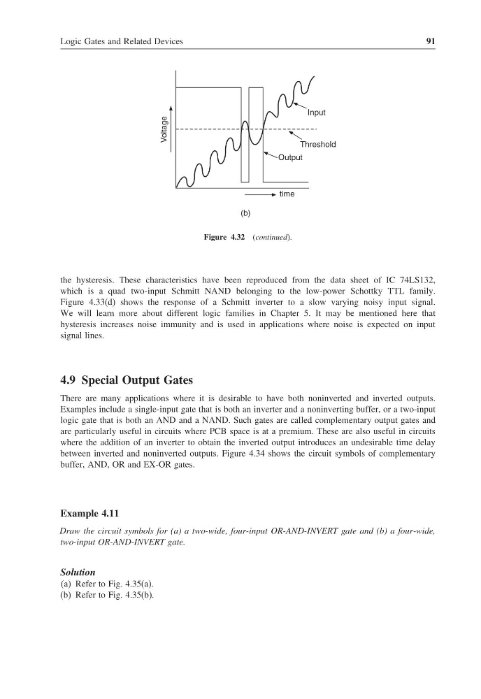
Figure 4.32 (continued).
the hysteresis. These characteristics have been reproduced from the data sheet of IC 74LS132,
which is a quad two-input Schmitt NAND belonging to the low-power Schottky TTL family.
Figure 4.33(d) shows the response of a Schmitt inverter to a slow varying noisy input signal.
We will learn more about different logic families in Chapter 5. It may be mentioned here that
hysteresis increases noise immunity and is used in applications where noise is expected on input
signal lines.
4.9 Special Output Gates
There are many applications where it is desirable to have both noninverted and inverted outputs.
Examples include a single-input gate that is both an inverter and a noninverting buffer, or a two-input
logic gate that is both an AND and a NAND. Such gates are called complementary output gates and
are particularly useful in circuits where PCB space is at a premium. These are also useful in circuits
where the addition of an inverter to obtain the inverted output introduces an undesirable time delay
between inverted and noninverted outputs. Figure 4.34 shows the circuit symbols of complementary
buffer, AND, OR and EX-OR gates.
Example 4.11
Draw the circuit symbols for (a) a two-wide, four-input OR-AND-INVERT gate and (b) a four-wide,
two-input OR-AND-INVERT gate.
Solution
(a) Refer to Fig. 4.35(a).
(b) Refer to Fig. 4.35(b).
91
Voltage
time
Input
Threshold
Output
(b)
Figure 4.32 (continued).
the hysteresis. These characteristics have been reproduced from the data sheet of IC 74LS132,
which is a quad two-input Schmitt NAND belonging to the low-power Schottky TTL family.
Figure 4.33(d) shows the response of a Schmitt inverter to a slow varying noisy input signal.
We will learn more about different logic families in Chapter 5. It may be mentioned here that
hysteresis increases noise immunity and is used in applications where noise is expected on input
signal lines.
4.9 Special Output Gates
There are many applications where it is desirable to have both noninverted and inverted outputs.
Examples include a single-input gate that is both an inverter and a noninverting buffer, or a two-input
logic gate that is both an AND and a NAND. Such gates are called complementary output gates and
are particularly useful in circuits where PCB space is at a premium. These are also useful in circuits
where the addition of an inverter to obtain the inverted output introduces an undesirable time delay
between inverted and noninverted outputs. Figure 4.34 shows the circuit symbols of complementary
buffer, AND, OR and EX-OR gates.
Example 4.11
Draw the circuit symbols for (a) a two-wide, four-input OR-AND-INVERT gate and (b) a four-wide,
two-input OR-AND-INVERT gate.
Solution
(a) Refer to Fig. 4.35(a).
(b) Refer to Fig. 4.35(b).