

board using photographic tools; holes are then drilled on the boards to create an
electric path between the layer and position to mount components. In this process,
the holes are subjected to etch-back process to remove smeared epoxy resin and
other contaminants using sulfuric or hydrochloric acids and potassium permanganate. Then, the holes are chemically plated with copper or graphite carbon and dried
for hours to prevent the board from rusting. The board is mechanically cleaned to
remove copper contaminants; it is chemically cleaned with alkaline acid and rinsed
water; the board is then set for electroless plating. The general steps involved in the
subtractive manufacturing process of Printed Wire Boards are board preparation,
application of conductive coating, soldering, fabrication, and assemblage.
Common materials used in the plating process are listed in Table 4.35.
The next step of the PWB production is imaging which involves photolithographic process. In this process, part of the board, where the circuit pattern will not
be set, is covered with photoresist; thereafter, it is developed after exposure to light,
to remove the resist layer on the unwanted areas. This is followed by light etching
using ammoniacal etchants to remove rust initiator and other metal, which is usually
copper. The board is then subjected to stencil printing process which is followed by
etching process, and thereafter, the photoresist is removed with photoresist stripper.
The next important step in the production of PWB is electroplating which is
employed to improve the electrical conductivity of the board and protection against
corrosion. Copper laminate is improved through photolithography and stenciling
processes to create the circuit pattern. Essentially, the PWB plating process involves
deposition of metals, particularly copper and tin-lead, in the plating bath to a
designed thickness; this is followed by etching or stripping processes. After this,
the board is thoroughly rinsed with water to end the chemical reactions and to
remove metal deposits and other impurities. The tin-lead layer is removed and the
panel conductivity is tested.
Soldering coating is another step in the manufacturing of PWB in which panel is
dipped into molten solder consisting of 60% tin and 40% lead. The required
thickness of the solder coat is between 50 and 1,200 microinches. Therefore, after
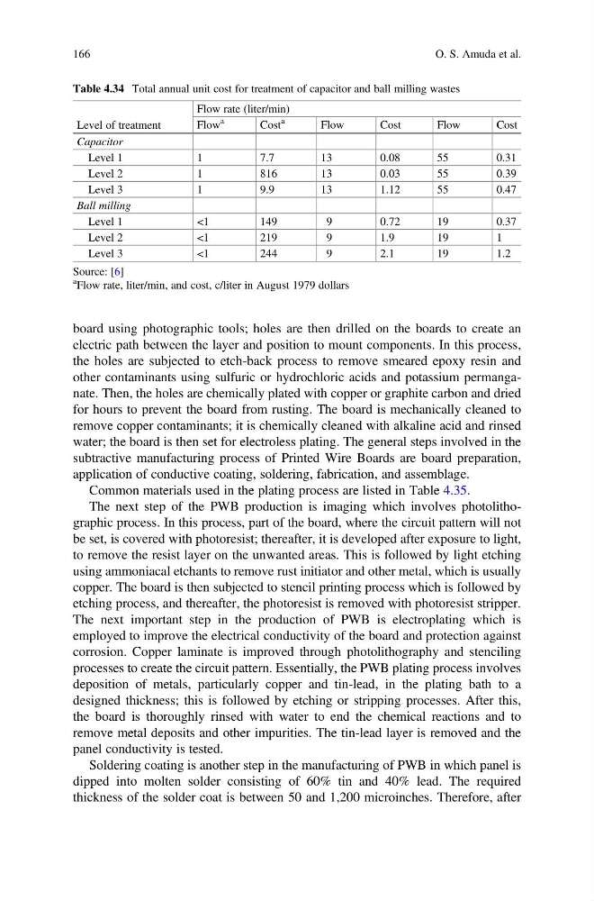
Table 4.34 Total annual unit cost for treatment of capacitor and ball milling wastes
Level of treatment
Flow rate (liter/min)
Flow
a
Cost
a
Flow
Cost
Flow
Cost
Capacitor
Level 1
1
7.7
13
0.08
55
0.31
Level 2
1
816
13
0.03
55
0.39
Level 3
1
9.9
13
1.12
55
0.47
Ball milling
Level 1
<1
149
9
0.72
19
0.37
Level 2
<1
219
9
1.9
19
1
Level 3
<1
244
9
2.1
19
1.2
Source: [6]
a Flow rate, liter/min, and cost, c/liter in August 1979 dollars
166
O. S. Amuda et al.
electric path between the layer and position to mount components. In this process,
the holes are subjected to etch-back process to remove smeared epoxy resin and
other contaminants using sulfuric or hydrochloric acids and potassium permanganate. Then, the holes are chemically plated with copper or graphite carbon and dried
for hours to prevent the board from rusting. The board is mechanically cleaned to
remove copper contaminants; it is chemically cleaned with alkaline acid and rinsed
water; the board is then set for electroless plating. The general steps involved in the
subtractive manufacturing process of Printed Wire Boards are board preparation,
application of conductive coating, soldering, fabrication, and assemblage.
Common materials used in the plating process are listed in Table 4.35.
The next step of the PWB production is imaging which involves photolithographic process. In this process, part of the board, where the circuit pattern will not
be set, is covered with photoresist; thereafter, it is developed after exposure to light,
to remove the resist layer on the unwanted areas. This is followed by light etching
using ammoniacal etchants to remove rust initiator and other metal, which is usually
copper. The board is then subjected to stencil printing process which is followed by
etching process, and thereafter, the photoresist is removed with photoresist stripper.
The next important step in the production of PWB is electroplating which is
employed to improve the electrical conductivity of the board and protection against
corrosion. Copper laminate is improved through photolithography and stenciling
processes to create the circuit pattern. Essentially, the PWB plating process involves
deposition of metals, particularly copper and tin-lead, in the plating bath to a
designed thickness; this is followed by etching or stripping processes. After this,
the board is thoroughly rinsed with water to end the chemical reactions and to
remove metal deposits and other impurities. The tin-lead layer is removed and the
panel conductivity is tested.
Soldering coating is another step in the manufacturing of PWB in which panel is
dipped into molten solder consisting of 60% tin and 40% lead. The required
thickness of the solder coat is between 50 and 1,200 microinches. Therefore, after
Table 4.34 Total annual unit cost for treatment of capacitor and ball milling wastes
Level of treatment
Flow rate (liter/min)
Flow
a
Cost
a
Flow
Cost
Flow
Cost
Capacitor
Level 1
1
7.7
13
0.08
55
0.31
Level 2
1
816
13
0.03
55
0.39
Level 3
1
9.9
13
1.12
55
0.47
Ball milling
Level 1
<1
149
9
0.72
19
0.37
Level 2
<1
219
9
1.9
19
1
Level 3
<1
244
9
2.1
19
1.2
Source: [6]
a Flow rate, liter/min, and cost, c/liter in August 1979 dollars
166
O. S. Amuda et al.