

Production of Silicon-Based ICs
Depending on types, purpose, and specifications, the intended semiconductors to be
used are first designed using all available engineering design aids ranging from
manual to software. This gives the viability of the semiconductors when tested with
computer simulation. Following fabrication of pattering “masks,” manufacturing
equipment is selected and operating conditions are set [20]. In the crystal processing
steps; silicon ingots are chemically doped through diffusion or ion implantation
process to produce silicon crystals with improved electrical conductivity and other
properties of semiconductors. Some of the doping materials (in either element or
compound forms) commonly used include antimony, arsenic, phosphorus, boron,
aluminum, gallium, germanium, tin, tellurium, and beryllium. Wafers are then
produced by slicing the ingots into cylindrical shapes of about 7.6 Â 10
À4 m
thickness and are etched mechanically and chemically. Etching generally facilitates
cutting into or imprinting on the surface material, which could be wet etching using
acid solution or dry etching involving reactive bases (halogenated or
non-halogenated gaseous compounds). Wafer fabrication involves oxidation step
in which a film of silicon dioxide is formed on the exterior surface of the silicon
wafer. Patterns are then imprinted onto the substrate through photolithography and
etching processes. Photolithography sets incorrect patterns affecting the electrical
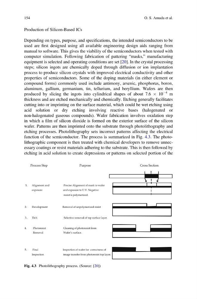
function of the semiconductor. The process is summarized in Fig. 4.3. The photolithographic component is then treated with chemical developers to remove unnecessary coatings or resist materials adhering to the substrate. This is then followed by
etching in acid solution to create depressions or patterns on selected portion of the
Process Step
Purpose
Cross Section
1.
Alignment and
Precise Alignment of mask to wafer
exposure
and exposure to U.V. Negative
resist is polymerized.
2.
Development
Removal of unpolymerized resist
3..
Etch
Selective removal of top surface layer.
4.
Photoresist
Cleaning of photoresist from
Removal
Wafer’s surface.
5.
Final
Inspection of wafer for correctness of
Inspection
image transfer from photoresist top layer.
Fig. 4.3 Photolithography process. (Source: [20])
154
O. S. Amuda et al.
Depending on types, purpose, and specifications, the intended semiconductors to be
used are first designed using all available engineering design aids ranging from
manual to software. This gives the viability of the semiconductors when tested with
computer simulation. Following fabrication of pattering “masks,” manufacturing
equipment is selected and operating conditions are set [20]. In the crystal processing
steps; silicon ingots are chemically doped through diffusion or ion implantation
process to produce silicon crystals with improved electrical conductivity and other
properties of semiconductors. Some of the doping materials (in either element or
compound forms) commonly used include antimony, arsenic, phosphorus, boron,
aluminum, gallium, germanium, tin, tellurium, and beryllium. Wafers are then
produced by slicing the ingots into cylindrical shapes of about 7.6 Â 10
À4 m
thickness and are etched mechanically and chemically. Etching generally facilitates
cutting into or imprinting on the surface material, which could be wet etching using
acid solution or dry etching involving reactive bases (halogenated or
non-halogenated gaseous compounds). Wafer fabrication involves oxidation step
in which a film of silicon dioxide is formed on the exterior surface of the silicon
wafer. Patterns are then imprinted onto the substrate through photolithography and
etching processes. Photolithography sets incorrect patterns affecting the electrical
function of the semiconductor. The process is summarized in Fig. 4.3. The photolithographic component is then treated with chemical developers to remove unnecessary coatings or resist materials adhering to the substrate. This is then followed by
etching in acid solution to create depressions or patterns on selected portion of the
Process Step
Purpose
Cross Section
1.
Alignment and
Precise Alignment of mask to wafer
exposure
and exposure to U.V. Negative
resist is polymerized.
2.
Development
Removal of unpolymerized resist
3..
Etch
Selective removal of top surface layer.
4.
Photoresist
Cleaning of photoresist from
Removal
Wafer’s surface.
5.
Final
Inspection of wafer for correctness of
Inspection
image transfer from photoresist top layer.
Fig. 4.3 Photolithography process. (Source: [20])
154
O. S. Amuda et al.