

oxide layers. Thereafter, the wafer is rinsed by dropping in stripping solution in order
to remove unwanted photoresist before being dried.
Through diffusion or implantation process, dopants are applied to the surface of
the patterned wafer and additional layers of silicon may be applied to the wafer using
epitaxial growth or chemical vapor deposition techniques. Other materials applicable
in this process include silane, silicon tetrachloride, ammonia, nitrogen, and hydrogen. These steps may be repeated more than once in order to meet specifications. The
fourth general step involved in the production of semiconductors is layering and
cleaning; in this step, the surface of the patterned wafer is coated with thin layers of
metal through metallization process involving spluttering. High-vacuum evaporation
metals like aluminum, platinum, nickel, chromium, silver, and others can be used in
this process, and their layers facilitate circuit/conduction properties within the
finished semiconductor. As applied in the steps above, the metalized wafers are
photolitographed and etched using halogenated solvents or acid solutions to remove
unnecessary metal. Final layers of oxide of varying thickness is then applied over the
surface of the processed wafer to provide a protective coat which protects the
semiconductor from exterior influences like metal contacts. The semiconductor
may range in thickness through the passivation process. The surface of the layers
is rinsed in deionized water, and back of the wafer is mechanically ground to remove
unnecessary materials. In order to improve connection of lead to the bonding pads
during future processes and use, a film of gold is often applied to the back of the
wafer. In order to determine if the produced chips meet the designed specifications,
they are tested with alcohol compounds and cleaned with solvents like deionized
water, acetone, methanol, and isopropyl alcohol. In assembly stage, the processed
and certified chips are mounted unto a metal frame which connects them to lead and
enclose them against mechanical shock and defects liable from the surrounding.
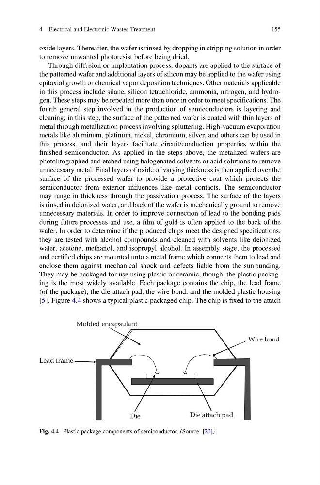
They may be packaged for use using plastic or ceramic, though, the plastic packaging is the most widely available. Each package contains the chip, the lead frame
(of the package), the die-attach pad, the wire bond, and the molded plastic housing
[5]. Figure 4.4 shows a typical plastic packaged chip. The chip is fixed to the attach
Die
Die attach pad
Wire bond
Lead frame
Molded encapsulant
Fig. 4.4 Plastic package components of semiconductor. (Source: [20])
4 Electrical and Electronic Wastes Treatment
155
to remove unwanted photoresist before being dried.
Through diffusion or implantation process, dopants are applied to the surface of
the patterned wafer and additional layers of silicon may be applied to the wafer using
epitaxial growth or chemical vapor deposition techniques. Other materials applicable
in this process include silane, silicon tetrachloride, ammonia, nitrogen, and hydrogen. These steps may be repeated more than once in order to meet specifications. The
fourth general step involved in the production of semiconductors is layering and
cleaning; in this step, the surface of the patterned wafer is coated with thin layers of
metal through metallization process involving spluttering. High-vacuum evaporation
metals like aluminum, platinum, nickel, chromium, silver, and others can be used in
this process, and their layers facilitate circuit/conduction properties within the
finished semiconductor. As applied in the steps above, the metalized wafers are
photolitographed and etched using halogenated solvents or acid solutions to remove
unnecessary metal. Final layers of oxide of varying thickness is then applied over the
surface of the processed wafer to provide a protective coat which protects the
semiconductor from exterior influences like metal contacts. The semiconductor
may range in thickness through the passivation process. The surface of the layers
is rinsed in deionized water, and back of the wafer is mechanically ground to remove
unnecessary materials. In order to improve connection of lead to the bonding pads
during future processes and use, a film of gold is often applied to the back of the
wafer. In order to determine if the produced chips meet the designed specifications,
they are tested with alcohol compounds and cleaned with solvents like deionized
water, acetone, methanol, and isopropyl alcohol. In assembly stage, the processed
and certified chips are mounted unto a metal frame which connects them to lead and
enclose them against mechanical shock and defects liable from the surrounding.
They may be packaged for use using plastic or ceramic, though, the plastic packaging is the most widely available. Each package contains the chip, the lead frame
(of the package), the die-attach pad, the wire bond, and the molded plastic housing
[5]. Figure 4.4 shows a typical plastic packaged chip. The chip is fixed to the attach
Die
Die attach pad
Wire bond
Lead frame
Molded encapsulant
Fig. 4.4 Plastic package components of semiconductor. (Source: [20])
4 Electrical and Electronic Wastes Treatment
155