

1 3
Topics in Current Chemistry (2020) 378:29
charge distribution, thereby shifting the Fermi level, leading to a more efficient
electron transfer in the system. The purpose of doping semiconductors is to create defect states in the band gap to enhance the interfacial charge transfer. These
defect states trap the VB holes and CB electrons, thereby inhibiting and retarding the recombination of holes and electrons. The type of dopant used is critical
in determining the overall activity of the photocatalysts. There have been multiple
reports on sonochemical synthesis of metal-doped TiO 2 . For example, Ambati and
Gogate [33] studied the synthesis of iron-doped TiO 2 catalyst using the ultrasoundbased approach and compared the efficacy of the ultrasound-assisted approach with
the conventional sol–gel method in terms of the difference in characteristics of the
obtained catalyst. Optimum synthesis conditions in terms of the irradiation time,
extent of doping, type of solvent and temperature were established. These authors
reported that the particle size obtained with the ultrasound-assisted approach was
99 nm and much smaller than that obtained with conventional approach, i.e. 325 nm
(see Fig. 6 for the particle size distribution data). The XRD analysis results reported
by these authors (see Fig. 7) allowed the doping efficacy to be established on the
basis of the diffraction peaks at a specific angle. More importantly, the crystallite
size for the catalyst obtained using the ultrasound-based approach (~ 25.4 nm) was
lower than that observed for the conventionally obtained catalyst (~ 31.2 nm). In
addition, the results of the scanning electron microscopy (SEM) analysis established
that the surface was more uniform, and the UV–Vis band gap energy estimations
demonstrated beneficial results for the ultrasound assisted approach [33]. In another
study, Stucchi et al. [34] demonstrated that ultrasound increased the loading of Ag
and Au onto the semiconductor surface. These authors reported that the deposition
of silver using the conventional method resulted in a narrow distribution of nanosized particles (typical range 0.5–3 nm) and that while the use of ultrasound did
not increase the dispersion, but it did provide a higher quantum of Ag being loaded.
The application of ultrasound induced the growth of Ag crystallites over the TiO 2
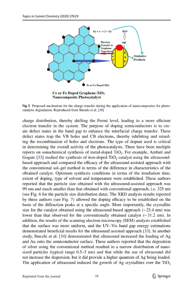
Fig. 5 Proposed mechanism for the charge transfer during the application of nanocomposites for photocatalytic degradation. Reproduced from Shende et al. [30]
79
Reprinted from the journal
Topics in Current Chemistry (2020) 378:29
charge distribution, thereby shifting the Fermi level, leading to a more efficient
electron transfer in the system. The purpose of doping semiconductors is to create defect states in the band gap to enhance the interfacial charge transfer. These
defect states trap the VB holes and CB electrons, thereby inhibiting and retarding the recombination of holes and electrons. The type of dopant used is critical
in determining the overall activity of the photocatalysts. There have been multiple
reports on sonochemical synthesis of metal-doped TiO 2 . For example, Ambati and
Gogate [33] studied the synthesis of iron-doped TiO 2 catalyst using the ultrasoundbased approach and compared the efficacy of the ultrasound-assisted approach with
the conventional sol–gel method in terms of the difference in characteristics of the
obtained catalyst. Optimum synthesis conditions in terms of the irradiation time,
extent of doping, type of solvent and temperature were established. These authors
reported that the particle size obtained with the ultrasound-assisted approach was
99 nm and much smaller than that obtained with conventional approach, i.e. 325 nm
(see Fig. 6 for the particle size distribution data). The XRD analysis results reported
by these authors (see Fig. 7) allowed the doping efficacy to be established on the
basis of the diffraction peaks at a specific angle. More importantly, the crystallite
size for the catalyst obtained using the ultrasound-based approach (~ 25.4 nm) was
lower than that observed for the conventionally obtained catalyst (~ 31.2 nm). In
addition, the results of the scanning electron microscopy (SEM) analysis established
that the surface was more uniform, and the UV–Vis band gap energy estimations
demonstrated beneficial results for the ultrasound assisted approach [33]. In another
study, Stucchi et al. [34] demonstrated that ultrasound increased the loading of Ag
and Au onto the semiconductor surface. These authors reported that the deposition
of silver using the conventional method resulted in a narrow distribution of nanosized particles (typical range 0.5–3 nm) and that while the use of ultrasound did
not increase the dispersion, but it did provide a higher quantum of Ag being loaded.
The application of ultrasound induced the growth of Ag crystallites over the TiO 2
Fig. 5 Proposed mechanism for the charge transfer during the application of nanocomposites for photocatalytic degradation. Reproduced from Shende et al. [30]
79
Reprinted from the journal