

The edge dislocation provides an insightful example
of a structure that can be modeled using the twodimensional plane strain form of the equilibrium
equations, (8.31)–(8.32), (Hirth and Lothe, 1982).
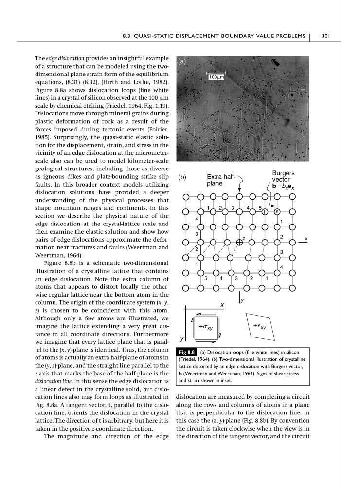
Figure 8.8a shows dislocation loops (fine white
lines) in a crystal of silicon observed at the 100-m
scale by chemical etching (Friedel, 1964, Fig. 1.19).
Dislocations move through mineral grains during
plastic deformation of rock as a result of the
forces imposed during tectonic events (Poirier,
1985). Surprisingly, the quasi-static elastic solution for the displacement, strain, and stress in the
vicinity of an edge dislocation at the micrometerscale also can be used to model kilometer-scale
geological structures, including those as diverse
as igneous dikes and plate-bounding strike slip
faults. In this broader context models utilizing
dislocation solutions have provided a deeper
understanding of the physical processes that
shape mountain ranges and continents. In this
section we describe the physical nature of the
edge dislocation at the crystal-lattice scale and
then examine the elastic solution and show how
pairs of edge dislocations approximate the deformation near fractures and faults (Weertman and
Weertman, 1964).
Figure 8.8b is a schematic two-dimensional
illustration of a crystalline lattice that contains
an edge dislocation. Note the extra column of
atoms that appears to distort locally the otherwise regular lattice near the bottom atom in the
column. The origin of the coordinate system (x, y,
z) is chosen to be coincident with this atom.
Although only a few atoms are illustrated, we
imagine the lattice extending a very great distance in all coordinate directions. Furthermore
we imagine that every lattice plane that is parallel to the (x, y)-plane is identical. Thus, the column
of atoms is actually an extra half-plane of atoms in
the (y, z)-plane, and the straight line parallel to the
z-axis that marks the base of the half-plane is the
dislocation line. In this sense the edge dislocation is
a linear defect in the crystalline solid, but dislocation lines also may form loops as illustrated in
Fig. 8.8a. A tangent vector, t, parallel to the dislocation line, orients the dislocation in the crystal
lattice. The direction of t is arbitrary, but here it is
taken in the positive z-coordinate direction.
The magnitude and direction of the edge
dislocation are measured by completing a circuit
along the rows and columns of atoms in a plane
that is perpendicular to the dislocation line, in
this case the (x, y)-plane (Fig. 8.8b). By convention
the circuit is taken clockwise when the view is in
the direction of the tangent vector, and the circuit
8.3 QUASI-STATIC DISPLACEMENT BOUNDARY VALUE PROBLEMS
301
Fig 8.8 (a) Dislocation loops (fine white lines) in silicon
(Friedel, 1964). (b) Two-dimensional illustration of crystalline
lattice distorted by an edge dislocation with Burgers vector,
b (Weertman and Weertman, 1964). Signs of shear stress
and strain shown in inset.
1
2
3
4
5
1
2
3
4
5
x
y
z
1
2
3
4
1
2
3
4
s
f
(b)
Extra halfplane
Burgers
vector
b = b x e x
(a)
x
y
+s xy
+e xy
100m
of a structure that can be modeled using the twodimensional plane strain form of the equilibrium
equations, (8.31)–(8.32), (Hirth and Lothe, 1982).
Figure 8.8a shows dislocation loops (fine white
lines) in a crystal of silicon observed at the 100-m
scale by chemical etching (Friedel, 1964, Fig. 1.19).
Dislocations move through mineral grains during
plastic deformation of rock as a result of the
forces imposed during tectonic events (Poirier,
1985). Surprisingly, the quasi-static elastic solution for the displacement, strain, and stress in the
vicinity of an edge dislocation at the micrometerscale also can be used to model kilometer-scale
geological structures, including those as diverse
as igneous dikes and plate-bounding strike slip
faults. In this broader context models utilizing
dislocation solutions have provided a deeper
understanding of the physical processes that
shape mountain ranges and continents. In this
section we describe the physical nature of the
edge dislocation at the crystal-lattice scale and
then examine the elastic solution and show how
pairs of edge dislocations approximate the deformation near fractures and faults (Weertman and
Weertman, 1964).
Figure 8.8b is a schematic two-dimensional
illustration of a crystalline lattice that contains
an edge dislocation. Note the extra column of
atoms that appears to distort locally the otherwise regular lattice near the bottom atom in the
column. The origin of the coordinate system (x, y,
z) is chosen to be coincident with this atom.
Although only a few atoms are illustrated, we
imagine the lattice extending a very great distance in all coordinate directions. Furthermore
we imagine that every lattice plane that is parallel to the (x, y)-plane is identical. Thus, the column
of atoms is actually an extra half-plane of atoms in
the (y, z)-plane, and the straight line parallel to the
z-axis that marks the base of the half-plane is the
dislocation line. In this sense the edge dislocation is
a linear defect in the crystalline solid, but dislocation lines also may form loops as illustrated in
Fig. 8.8a. A tangent vector, t, parallel to the dislocation line, orients the dislocation in the crystal
lattice. The direction of t is arbitrary, but here it is
taken in the positive z-coordinate direction.
The magnitude and direction of the edge
dislocation are measured by completing a circuit
along the rows and columns of atoms in a plane
that is perpendicular to the dislocation line, in
this case the (x, y)-plane (Fig. 8.8b). By convention
the circuit is taken clockwise when the view is in
the direction of the tangent vector, and the circuit
8.3 QUASI-STATIC DISPLACEMENT BOUNDARY VALUE PROBLEMS
301
Fig 8.8 (a) Dislocation loops (fine white lines) in silicon
(Friedel, 1964). (b) Two-dimensional illustration of crystalline
lattice distorted by an edge dislocation with Burgers vector,
b (Weertman and Weertman, 1964). Signs of shear stress
and strain shown in inset.
1
2
3
4
5
1
2
3
4
5
x
y
z
1
2
3
4
1
2
3
4
s
f
(b)
Extra halfplane
Burgers
vector
b = b x e x
(a)
x
y
+s xy
+e xy
100m