

E ξ ¼ Ài
γ
ωε 0 e n
2
e
He
γζ and E ξ ¼ i
γ
ωε 0 e n
2
e
He
Àγ ζÀ
d
cos δ
ð
Þ
ð9:129Þ
for the substrate and air, respectively.
The device geometry is characterized by that the P6T slab crystal is sandwiched
by air and the device substrate so as to form the three-layered (air/crystal/substrate)
structure (Fig. 9.10c). Therefore, we impose boundary conditions on H η in (9.119)
and (9.128) along with E ξ in (9.123) and (9.129) in such a way that their tangential
components are continuous across the interfaces between the crystal and the substrate and between the crystal and air.
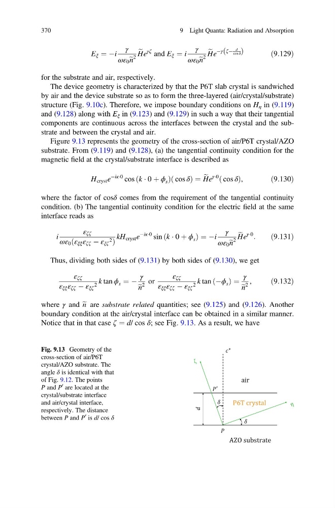
Figure 9.13 represents the geometry of the cross-section of air/P6T crystal/AZO
substrate. From (9.119) and (9.128), (a) the tangential continuity condition for the
magnetic field at the crystal/substrate interface is described as
H cryst e
ÀiκÁ0 cos k Á 0 þ ϕ s
ð
Þ cos δ
ð
Þ¼ e
He
γÁ0 cos δ
ð
Þ,
ð9:130Þ
where the factor of cosδ comes from the requirement of the tangential continuity
condition. (b) The tangential continuity condition for the electric field at the same
interface reads as
i
ε ζζ
ωε 0 ε ξξ ε ζζ À ε ξζ
2
ð
Þ
kH cryst e
ÀiκÁ0 sin k Á 0 þ ϕ s
ð
Þ¼À i
γ
ωε 0 e n
2
e
He
γÁ0
:
ð9:131Þ
Thus, dividing both sides of (9.131) by both sides of (9.130), we get
ε ζζ
ε ξξ ε ζζ À ε ξζ
2
k tan ϕ s ¼ À
γ
e n
2
or
ε ζζ
ε ξξ ε ζζ À ε ξζ
2
k tan Àϕ s
ð
Þ ¼
γ
e n
2
,
ð9:132Þ
where γ and e n are substrate related quantities; see (9.125) and (9.126). Another
boundary condition at the air/crystal interface can be obtained in a similar manner.
Notice that in that case ζ ¼ d/ cos δ; see Fig. 9.13. As a result, we have
∗
air
P6T crystal
AZO substrate
Fig. 9.13 Geometry of the
cross-section of air/P6T
crystal/AZO substrate. The
angle δ is identical with that
of Fig. 9.12. The points
P and P
0 are located at the
crystal/substrate interface
and air/crystal interface,
respectively. The distance
between P and P
0 is d/ cos δ
370
9 Light Quanta: Radiation and Absorption
γ
ωε 0 e n
2
e
He
γζ and E ξ ¼ i
γ
ωε 0 e n
2
e
He
Àγ ζÀ
d
cos δ
ð
Þ
ð9:129Þ
for the substrate and air, respectively.
The device geometry is characterized by that the P6T slab crystal is sandwiched
by air and the device substrate so as to form the three-layered (air/crystal/substrate)
structure (Fig. 9.10c). Therefore, we impose boundary conditions on H η in (9.119)
and (9.128) along with E ξ in (9.123) and (9.129) in such a way that their tangential
components are continuous across the interfaces between the crystal and the substrate and between the crystal and air.
Figure 9.13 represents the geometry of the cross-section of air/P6T crystal/AZO
substrate. From (9.119) and (9.128), (a) the tangential continuity condition for the
magnetic field at the crystal/substrate interface is described as
H cryst e
ÀiκÁ0 cos k Á 0 þ ϕ s
ð
Þ cos δ
ð
Þ¼ e
He
γÁ0 cos δ
ð
Þ,
ð9:130Þ
where the factor of cosδ comes from the requirement of the tangential continuity
condition. (b) The tangential continuity condition for the electric field at the same
interface reads as
i
ε ζζ
ωε 0 ε ξξ ε ζζ À ε ξζ
2
ð
Þ
kH cryst e
ÀiκÁ0 sin k Á 0 þ ϕ s
ð
Þ¼À i
γ
ωε 0 e n
2
e
He
γÁ0
:
ð9:131Þ
Thus, dividing both sides of (9.131) by both sides of (9.130), we get
ε ζζ
ε ξξ ε ζζ À ε ξζ
2
k tan ϕ s ¼ À
γ
e n
2
or
ε ζζ
ε ξξ ε ζζ À ε ξζ
2
k tan Àϕ s
ð
Þ ¼
γ
e n
2
,
ð9:132Þ
where γ and e n are substrate related quantities; see (9.125) and (9.126). Another
boundary condition at the air/crystal interface can be obtained in a similar manner.
Notice that in that case ζ ¼ d/ cos δ; see Fig. 9.13. As a result, we have
∗
air
P6T crystal
AZO substrate
Fig. 9.13 Geometry of the
cross-section of air/P6T
crystal/AZO substrate. The
angle δ is identical with that
of Fig. 9.12. The points
P and P
0 are located at the
crystal/substrate interface
and air/crystal interface,
respectively. The distance
between P and P
0 is d/ cos δ
370
9 Light Quanta: Radiation and Absorption