

alternating bias voltage is applied to it. Hence, upper plate is now negatively
charges and respective bottom plate becomes positively charged; and an electric
field is setup between the two.
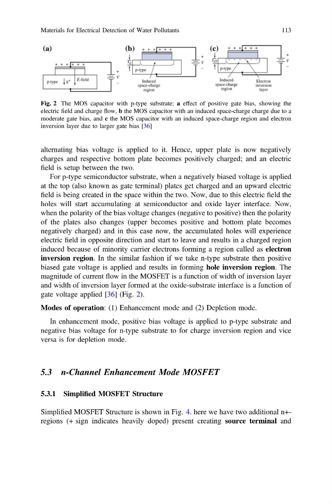
For p-type semiconductor substrate, when a negatively biased voltage is applied
at the top (also known as gate terminal) plates get charged and an upward electric
field is being created in the space within the two. Now, due to this electric field the
holes will start accumulating at semiconductor and oxide layer interface. Now,
when the polarity of the bias voltage changes (negative to positive) then the polarity
of the plates also changes (upper becomes positive and bottom plate becomes
negatively charged) and in this case now, the accumulated holes will experience
electric field in opposite direction and start to leave and results in a charged region
induced because of minority carrier electrons forming a region called as electron
inversion region. In the similar fashion if we take n-type substrate then positive
biased gate voltage is applied and results in forming hole inversion region. The
magnitude of current flow in the MOSFET is a function of width of inversion layer
and width of inversion layer formed at the oxide-substrate interface is a function of
gate voltage applied [36] (Fig. 2).
Modes of operation: (1) Enhancement mode and (2) Depletion mode.
In enhancement mode, positive bias voltage is applied to p-type substrate and
negative bias voltage for n-type substrate to for charge inversion region and vice
versa is for depletion mode.
5.3 n-Channel Enhancement Mode MOSFET
5.3.1 Simplified MOSFET Structure
Simplified MOSFET Structure is shown in Fig. 4. here we have two additional n+regions (+ sign indicates heavily doped) present creating source terminal and
Fig. 2 The MOS capacitor with p-type substrate: a effect of positive gate bias, showing the
electric field and charge flow, b the MOS capacitor with an induced space-charge charge due to a
moderate gate bias, and c the MOS capacitor with an induced space-charge region and electron
inversion layer due to larger gate bias [36]
Materials for Electrical Detection of Water Pollutants
113
charges and respective bottom plate becomes positively charged; and an electric
field is setup between the two.
For p-type semiconductor substrate, when a negatively biased voltage is applied
at the top (also known as gate terminal) plates get charged and an upward electric
field is being created in the space within the two. Now, due to this electric field the
holes will start accumulating at semiconductor and oxide layer interface. Now,
when the polarity of the bias voltage changes (negative to positive) then the polarity
of the plates also changes (upper becomes positive and bottom plate becomes
negatively charged) and in this case now, the accumulated holes will experience
electric field in opposite direction and start to leave and results in a charged region
induced because of minority carrier electrons forming a region called as electron
inversion region. In the similar fashion if we take n-type substrate then positive
biased gate voltage is applied and results in forming hole inversion region. The
magnitude of current flow in the MOSFET is a function of width of inversion layer
and width of inversion layer formed at the oxide-substrate interface is a function of
gate voltage applied [36] (Fig. 2).
Modes of operation: (1) Enhancement mode and (2) Depletion mode.
In enhancement mode, positive bias voltage is applied to p-type substrate and
negative bias voltage for n-type substrate to for charge inversion region and vice
versa is for depletion mode.
5.3 n-Channel Enhancement Mode MOSFET
5.3.1 Simplified MOSFET Structure
Simplified MOSFET Structure is shown in Fig. 4. here we have two additional n+regions (+ sign indicates heavily doped) present creating source terminal and
Fig. 2 The MOS capacitor with p-type substrate: a effect of positive gate bias, showing the
electric field and charge flow, b the MOS capacitor with an induced space-charge charge due to a
moderate gate bias, and c the MOS capacitor with an induced space-charge region and electron
inversion layer due to larger gate bias [36]
Materials for Electrical Detection of Water Pollutants
113