

drain terminal. The current flow through inversion layer is termed as channel
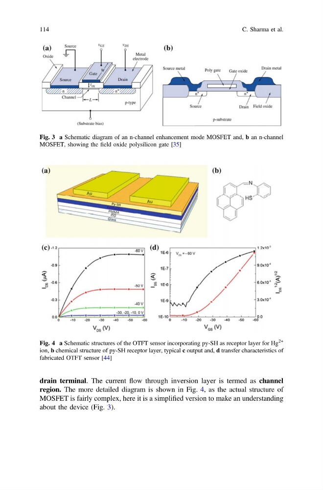
region. The more detailed diagram is shown in Fig. 4, as the actual structure of
MOSFET is fairly complex, here it is a simplified version to make an understanding
about the device (Fig. 3).
Fig. 3 a Schematic diagram of an n-channel enhancement mode MOSFET and, b an n-channel
MOSFET, showing the field oxide polysilicon gate [35]
Fig. 4 a Schematic structures of the OTFT sensor incorporating py-SH as receptor layer for Hg
2+
ion, b chemical structure of py-SH receptor layer, typical c output and, d transfer characteristics of
fabricated OTFT sensor [44]
114
C. Sharma et al.
region. The more detailed diagram is shown in Fig. 4, as the actual structure of
MOSFET is fairly complex, here it is a simplified version to make an understanding
about the device (Fig. 3).
Fig. 3 a Schematic diagram of an n-channel enhancement mode MOSFET and, b an n-channel
MOSFET, showing the field oxide polysilicon gate [35]
Fig. 4 a Schematic structures of the OTFT sensor incorporating py-SH as receptor layer for Hg
2+
ion, b chemical structure of py-SH receptor layer, typical c output and, d transfer characteristics of
fabricated OTFT sensor [44]
114
C. Sharma et al.