

13 Some Frontier Technologies for Aptamers in Medical Applications
395
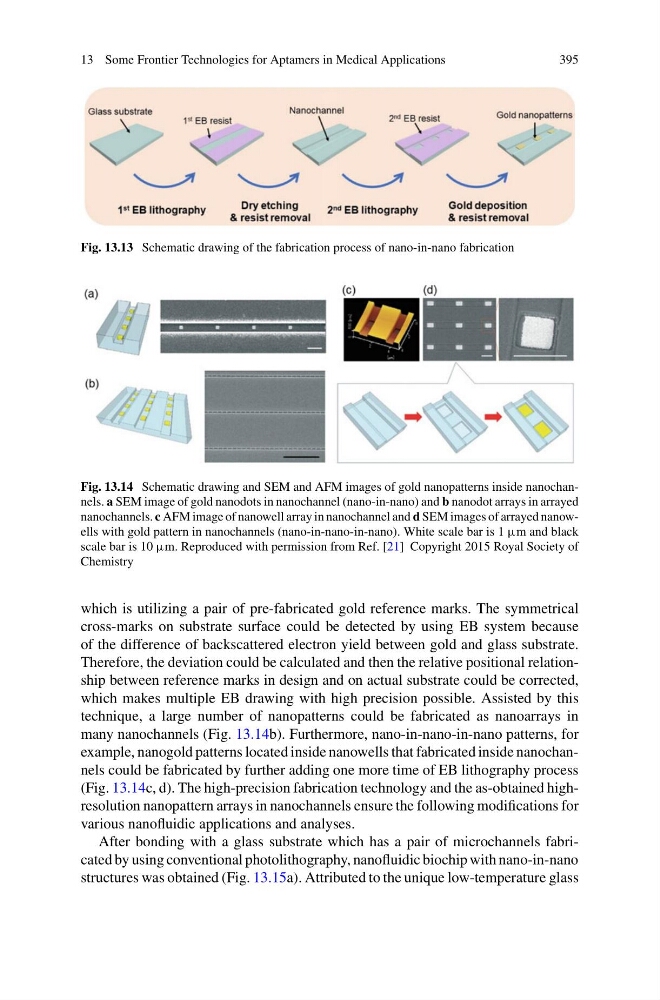
Fig. 13.13 Schematic drawing of the fabrication process of nano-in-nano fabrication
Fig. 13.14 Schematic drawing and SEM and AFM images of gold nanopatterns inside nanochannels. a SEM image of gold nanodots in nanochannel (nano-in-nano) and b nanodot arrays in arrayed
nanochannels. c AFM image of nanowell array in nanochannel and d SEM images of arrayed nanowells with gold pattern in nanochannels (nano-in-nano-in-nano). White scale bar is 1 µm and black
scale bar is 10 µm. Reproduced with permission from Ref. [21] Copyright 2015 Royal Society of
Chemistry
which is utilizing a pair of pre-fabricated gold reference marks. The symmetrical
cross-marks on substrate surface could be detected by using EB system because
of the difference of backscattered electron yield between gold and glass substrate.
Therefore, the deviation could be calculated and then the relative positional relationship between reference marks in design and on actual substrate could be corrected,
which makes multiple EB drawing with high precision possible. Assisted by this
technique, a large number of nanopatterns could be fabricated as nanoarrays in
many nanochannels (Fig. 13.14b). Furthermore, nano-in-nano-in-nano patterns, for
example, nanogold patterns located inside nanowells that fabricated inside nanochannels could be fabricated by further adding one more time of EB lithography process
(Fig. 13.14c, d). The high-precision fabrication technology and the as-obtained highresolution nanopattern arrays in nanochannels ensure the following modifications for
various nanofluidic applications and analyses.
After bonding with a glass substrate which has a pair of microchannels fabricated by using conventional photolithography, nanofluidic biochip with nano-in-nano
structures was obtained (Fig. 13.15a). Attributed to the unique low-temperature glass
395
Fig. 13.13 Schematic drawing of the fabrication process of nano-in-nano fabrication
Fig. 13.14 Schematic drawing and SEM and AFM images of gold nanopatterns inside nanochannels. a SEM image of gold nanodots in nanochannel (nano-in-nano) and b nanodot arrays in arrayed
nanochannels. c AFM image of nanowell array in nanochannel and d SEM images of arrayed nanowells with gold pattern in nanochannels (nano-in-nano-in-nano). White scale bar is 1 µm and black
scale bar is 10 µm. Reproduced with permission from Ref. [21] Copyright 2015 Royal Society of
Chemistry
which is utilizing a pair of pre-fabricated gold reference marks. The symmetrical
cross-marks on substrate surface could be detected by using EB system because
of the difference of backscattered electron yield between gold and glass substrate.
Therefore, the deviation could be calculated and then the relative positional relationship between reference marks in design and on actual substrate could be corrected,
which makes multiple EB drawing with high precision possible. Assisted by this
technique, a large number of nanopatterns could be fabricated as nanoarrays in
many nanochannels (Fig. 13.14b). Furthermore, nano-in-nano-in-nano patterns, for
example, nanogold patterns located inside nanowells that fabricated inside nanochannels could be fabricated by further adding one more time of EB lithography process
(Fig. 13.14c, d). The high-precision fabrication technology and the as-obtained highresolution nanopattern arrays in nanochannels ensure the following modifications for
various nanofluidic applications and analyses.
After bonding with a glass substrate which has a pair of microchannels fabricated by using conventional photolithography, nanofluidic biochip with nano-in-nano
structures was obtained (Fig. 13.15a). Attributed to the unique low-temperature glass