

394
Y. Dong et al.
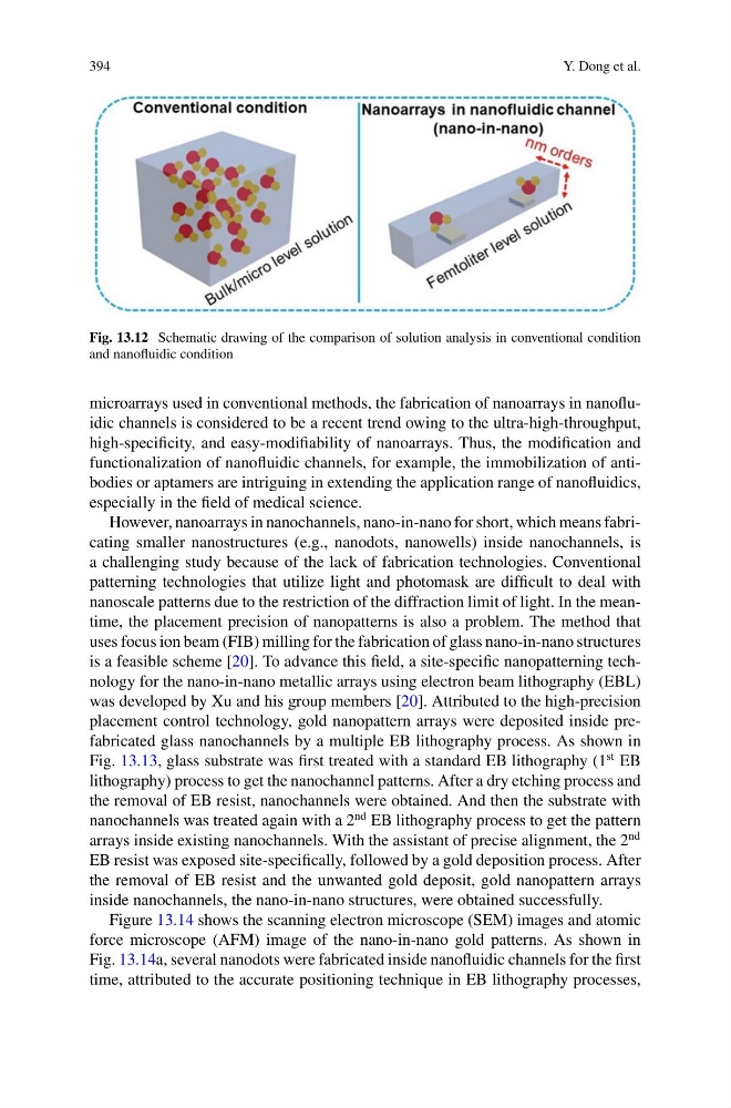
Fig. 13.12 Schematic drawing of the comparison of solution analysis in conventional condition
and nanofluidic condition
microarrays used in conventional methods, the fabrication of nanoarrays in nanofluidic channels is considered to be a recent trend owing to the ultra-high-throughput,
high-specificity, and easy-modifiability of nanoarrays. Thus, the modification and
functionalization of nanofluidic channels, for example, the immobilization of antibodies or aptamers are intriguing in extending the application range of nanofluidics,
especially in the field of medical science.
However, nanoarrays in nanochannels, nano-in-nano for short, which means fabricating smaller nanostructures (e.g., nanodots, nanowells) inside nanochannels, is
a challenging study because of the lack of fabrication technologies. Conventional
patterning technologies that utilize light and photomask are difficult to deal with
nanoscale patterns due to the restriction of the diffraction limit of light. In the meantime, the placement precision of nanopatterns is also a problem. The method that
uses focus ion beam (FIB) milling for the fabrication of glass nano-in-nano structures
is a feasible scheme [20]. To advance this field, a site-specific nanopatterning technology for the nano-in-nano metallic arrays using electron beam lithography (EBL)
was developed by Xu and his group members [20]. Attributed to the high-precision
placement control technology, gold nanopattern arrays were deposited inside prefabricated glass nanochannels by a multiple EB lithography process. As shown in
Fig. 13.13, glass substrate was first treated with a standard EB lithography (1
st EB
lithography) process to get the nanochannel patterns. After a dry etching process and
the removal of EB resist, nanochannels were obtained. And then the substrate with
nanochannels was treated again with a 2
nd EB lithography process to get the pattern
arrays inside existing nanochannels. With the assistant of precise alignment, the 2
nd
EB resist was exposed site-specifically, followed by a gold deposition process. After
the removal of EB resist and the unwanted gold deposit, gold nanopattern arrays
inside nanochannels, the nano-in-nano structures, were obtained successfully.
Figure 13.14 shows the scanning electron microscope (SEM) images and atomic
force microscope (AFM) image of the nano-in-nano gold patterns. As shown in
Fig. 13.14a, several nanodots were fabricated inside nanofluidic channels for the first
time, attributed to the accurate positioning technique in EB lithography processes,
Y. Dong et al.
Fig. 13.12 Schematic drawing of the comparison of solution analysis in conventional condition
and nanofluidic condition
microarrays used in conventional methods, the fabrication of nanoarrays in nanofluidic channels is considered to be a recent trend owing to the ultra-high-throughput,
high-specificity, and easy-modifiability of nanoarrays. Thus, the modification and
functionalization of nanofluidic channels, for example, the immobilization of antibodies or aptamers are intriguing in extending the application range of nanofluidics,
especially in the field of medical science.
However, nanoarrays in nanochannels, nano-in-nano for short, which means fabricating smaller nanostructures (e.g., nanodots, nanowells) inside nanochannels, is
a challenging study because of the lack of fabrication technologies. Conventional
patterning technologies that utilize light and photomask are difficult to deal with
nanoscale patterns due to the restriction of the diffraction limit of light. In the meantime, the placement precision of nanopatterns is also a problem. The method that
uses focus ion beam (FIB) milling for the fabrication of glass nano-in-nano structures
is a feasible scheme [20]. To advance this field, a site-specific nanopatterning technology for the nano-in-nano metallic arrays using electron beam lithography (EBL)
was developed by Xu and his group members [20]. Attributed to the high-precision
placement control technology, gold nanopattern arrays were deposited inside prefabricated glass nanochannels by a multiple EB lithography process. As shown in
Fig. 13.13, glass substrate was first treated with a standard EB lithography (1
st EB
lithography) process to get the nanochannel patterns. After a dry etching process and
the removal of EB resist, nanochannels were obtained. And then the substrate with
nanochannels was treated again with a 2
nd EB lithography process to get the pattern
arrays inside existing nanochannels. With the assistant of precise alignment, the 2
nd
EB resist was exposed site-specifically, followed by a gold deposition process. After
the removal of EB resist and the unwanted gold deposit, gold nanopattern arrays
inside nanochannels, the nano-in-nano structures, were obtained successfully.
Figure 13.14 shows the scanning electron microscope (SEM) images and atomic
force microscope (AFM) image of the nano-in-nano gold patterns. As shown in
Fig. 13.14a, several nanodots were fabricated inside nanofluidic channels for the first
time, attributed to the accurate positioning technique in EB lithography processes,