

15 Super-Resolution Imaging and Microscopy by Dielectric …
393
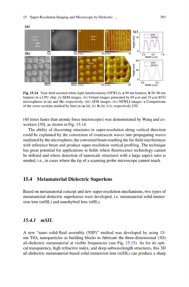
Fig. 15.14 Near-field assisted white-light interferometry (NFWLI). a 90 nm features, b 20–90 nm
features in a CPU chip. (i) SEM images. (ii) Virtual images generated by 69 μm and 19 μm BTG
microspheres in (a) and (b), respectively. (iii) AFM images. (iv) NFWLI images. c Comparisons
of the cross-sections marked by lines in (a (iii, iv)–b (iii, iv)), respectively [39]
(40 times faster than atomic force microscopes) was demonstrated by Wang and coworkers [39], as shown in Fig. 15.14.
The ability of discerning structures in super-resolution along vertical direction
could be explained by the conversion of evanescent waves into propagating waves
mediated by the microsphere; the converted beam reaching the far-field interferences
with reference beam and produce super-resolution vertical profiling. The technique
has great potential for applications in fields where fluorescence technology cannot
be utilized and where detection of nanoscale structures with a large aspect ratio is
needed, i.e., in cases where the tip of a scanning probe microscope cannot reach.
15.4 Metamaterial Dielectric Superlens
Based on metamaterial concept and new super-resolution mechanisms, two types of
metamaterial dielectric superlenses were developed, i.e. metamaterial solid immersion lens (mSIL) and nanohybrid lens (nHL).
15.4.1 mSIL
A new “nano–solid-fluid assembly (NSF)” method was developed by using 15nm TiO 2 nanoparticles as building blocks to fabricate the three-dimensional (3D)
all-dielectric metamaterial at visible frequencies (see Fig. 15.15). As for its optical transparency, high refractive index, and deep-subwavelength structures, this 3D
all-dielectric metamaterial-based solid immersion lens (mSIL) can produce a sharp
393
Fig. 15.14 Near-field assisted white-light interferometry (NFWLI). a 90 nm features, b 20–90 nm
features in a CPU chip. (i) SEM images. (ii) Virtual images generated by 69 μm and 19 μm BTG
microspheres in (a) and (b), respectively. (iii) AFM images. (iv) NFWLI images. c Comparisons
of the cross-sections marked by lines in (a (iii, iv)–b (iii, iv)), respectively [39]
(40 times faster than atomic force microscopes) was demonstrated by Wang and coworkers [39], as shown in Fig. 15.14.
The ability of discerning structures in super-resolution along vertical direction
could be explained by the conversion of evanescent waves into propagating waves
mediated by the microsphere; the converted beam reaching the far-field interferences
with reference beam and produce super-resolution vertical profiling. The technique
has great potential for applications in fields where fluorescence technology cannot
be utilized and where detection of nanoscale structures with a large aspect ratio is
needed, i.e., in cases where the tip of a scanning probe microscope cannot reach.
15.4 Metamaterial Dielectric Superlens
Based on metamaterial concept and new super-resolution mechanisms, two types of
metamaterial dielectric superlenses were developed, i.e. metamaterial solid immersion lens (mSIL) and nanohybrid lens (nHL).
15.4.1 mSIL
A new “nano–solid-fluid assembly (NSF)” method was developed by using 15nm TiO 2 nanoparticles as building blocks to fabricate the three-dimensional (3D)
all-dielectric metamaterial at visible frequencies (see Fig. 15.15). As for its optical transparency, high refractive index, and deep-subwavelength structures, this 3D
all-dielectric metamaterial-based solid immersion lens (mSIL) can produce a sharp