

11 Label-Free Super-Resolution Microscopy by Nonlinear …
269
11.4 Examples of NPMR
11.4.1 Silicon on Sapphire
We first demonstrated SR using NPMR on fabricated silicon nanostructures. In silicon
nanostructures, the major material in semiconductor industry, linear photo-modulated
reflection has been studied extensively. Silicon, as any other reflective or scattering
surface, contains nonlinear components in its reflectivity [25–27].
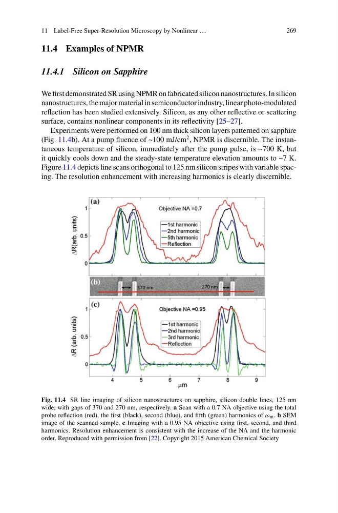
Experiments were performed on 100 nm thick silicon layers patterned on sapphire
(Fig. 11.4b). At a pump fluence of ~100 mJ/cm
2 , NPMR is discernible. The instantaneous temperature of silicon, immediately after the pump pulse, is ~700 K, but
it quickly cools down and the steady-state temperature elevation amounts to ~7 K.
Figure 11.4 depicts line scans orthogonal to 125 nm silicon stripes with variable spacing. The resolution enhancement with increasing harmonics is clearly discernible.
Fig. 11.4 SR line imaging of silicon nanostructures on sapphire, silicon double lines, 125 nm
wide, with gaps of 370 and 270 nm, respectively. a Scan with a 0.7 NA objective using the total
probe reflection (red), the first (black), second (blue), and fifth (green) harmonics of ω m . b SEM
image of the scanned sample. c Imaging with a 0.95 NA objective using first, second, and third
harmonics. Resolution enhancement is consistent with the increase of the NA and the harmonic
order. Reproduced with permission from [22]. Copyright 2015 American Chemical Society
269
11.4 Examples of NPMR
11.4.1 Silicon on Sapphire
We first demonstrated SR using NPMR on fabricated silicon nanostructures. In silicon
nanostructures, the major material in semiconductor industry, linear photo-modulated
reflection has been studied extensively. Silicon, as any other reflective or scattering
surface, contains nonlinear components in its reflectivity [25–27].
Experiments were performed on 100 nm thick silicon layers patterned on sapphire
(Fig. 11.4b). At a pump fluence of ~100 mJ/cm
2 , NPMR is discernible. The instantaneous temperature of silicon, immediately after the pump pulse, is ~700 K, but
it quickly cools down and the steady-state temperature elevation amounts to ~7 K.
Figure 11.4 depicts line scans orthogonal to 125 nm silicon stripes with variable spacing. The resolution enhancement with increasing harmonics is clearly discernible.
Fig. 11.4 SR line imaging of silicon nanostructures on sapphire, silicon double lines, 125 nm
wide, with gaps of 370 and 270 nm, respectively. a Scan with a 0.7 NA objective using the total
probe reflection (red), the first (black), second (blue), and fifth (green) harmonics of ω m . b SEM
image of the scanned sample. c Imaging with a 0.95 NA objective using first, second, and third
harmonics. Resolution enhancement is consistent with the increase of the NA and the harmonic
order. Reproduced with permission from [22]. Copyright 2015 American Chemical Society