

9 Usage of Silicon for Label-Free Super-Resolved Imaging
225
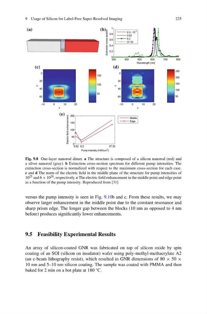
Fig. 9.8 One-layer nanorod dimer. a The structure is composed of a silicon nanorod (red) and
a silver nanorod (gray). b Extinction cross-section spectrum for different pump intensities. The
extinction cross-section is normalized with respect to the maximum cross-section for each case.
c and d The norm of the electric field in the middle plane of the structure for pump intensities of
10 25 and 6 × 10 28 , respectively. e The electric field enhancement in the middle point and edge point
as a function of the pump intensity. Reproduced from [31]
versus the pump intensity is seen in Fig. 9.10b and c. From these results, we may
observe larger enhancement in the middle point due to the constant resonance and
sharp prism edge. The longer gap between the blocks (10 nm as opposed to 4 nm
before) produces significantly lower enhancements.
9.5 Feasibility Experimental Results
An array of silicon-coated GNR was fabricated on top of silicon oxide by spin
coating of an SOI (silicon on insulator) wafer using poly-methyl-methacrylate A2
(an e-beam lithography resist), which resulted in GNR dimensions of 80 × 50 ×
10 nm and 5–10 nm silicon coating. The sample was coated with PMMA and then
baked for 2 min on a hot plate at 180 °C.
225
Fig. 9.8 One-layer nanorod dimer. a The structure is composed of a silicon nanorod (red) and
a silver nanorod (gray). b Extinction cross-section spectrum for different pump intensities. The
extinction cross-section is normalized with respect to the maximum cross-section for each case.
c and d The norm of the electric field in the middle plane of the structure for pump intensities of
10 25 and 6 × 10 28 , respectively. e The electric field enhancement in the middle point and edge point
as a function of the pump intensity. Reproduced from [31]
versus the pump intensity is seen in Fig. 9.10b and c. From these results, we may
observe larger enhancement in the middle point due to the constant resonance and
sharp prism edge. The longer gap between the blocks (10 nm as opposed to 4 nm
before) produces significantly lower enhancements.
9.5 Feasibility Experimental Results
An array of silicon-coated GNR was fabricated on top of silicon oxide by spin
coating of an SOI (silicon on insulator) wafer using poly-methyl-methacrylate A2
(an e-beam lithography resist), which resulted in GNR dimensions of 80 × 50 ×
10 nm and 5–10 nm silicon coating. The sample was coated with PMMA and then
baked for 2 min on a hot plate at 180 °C.