

5 Near-Field Scanning Optical Microscope Combined with Digital …
123
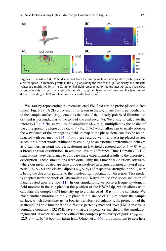
Fig. 5.7 Reconstructed EM field scattered from the hollow metal-coated aperture probe placed in
air (free space). b Intensity profile in the x–z plane along the axis of the tip. For clarity, the intensity
values are multiplied by ρ 2 . c Complex EM field represented by the product ρ|A(x, y, z)|cos(φ(x,
y, z)), where A(x, y, z) is the amplitude, and φ(x, y, z) the phase. Wavefronts are clearly observed.
d Corresponding FDTD simulated intensity multiplied by ρ 2
We start by representing the reconstructed EM field for the probe placed in free
space (Fig. 5.7a). A 2D cross-section is taken in the x–z plane that is perpendicular
to the sample surface (x–y), contains the axis of the linearly polarized illumination
(x), and is perpendicular to the axis of the cantilever (y). We chose to calculate the
intensity (Fig. 5.7b), as well as the amplitude |A(x, y, z)| multiplied by the cosine of
the corresponding phase cos φ(x, y, z) (Fig. 5.7c) which allows us to easily observe
the wavefronts of the propagating field. A map of the phase alone can also be reconstructed with our method [34]. From these results, we infer that a tip placed in free
space, or in other words, without any coupling to an external environment, behaves
as a Lambertian point source, scattering an EM field centered about θ = 0° with
a broad angular distribution. In addition, Finite Difference Time-Domain (FDTD)
simulations were performed to compare these experimental results to the theoretical
description. Those simulations were done using the Lumerical Solutions software,
where our metal-coated aperture probe is modeled as a superposition of lateral magnetic (M y ∝ H y ) and electric dipoles (P x ∝ E x ) of respective strengths 2 and 1, with
x being the direction parallel to the incident light polarization direction. This model
is adapted from the work of Obermüller and Karrai on the free space radiation of
metal coated aperture tips [11]. In our simulations, we place a frequency-domain
field monitor in the x–z plane at the position of the NSOM tip, which allows us to
calculate the complex EM intensity up to a distance of 10 μm in the substrate. We
place another monitor in the x–y plane at a distance of 10 μm below the sample
surface, which determines using Fourier transform calculations, the projection of the
scattered EM field into the far field. We use perfectly matched layer (PML) absorbing
boundary conditions (32 PML layers) that are impedance-matched to the simulation
region and its materials, and the value of the complex permittivity of gold is ε gold = −
12.047 + 1.163i at 633 nm, taken from Olmon et al. [40]. It is important to note here
123
Fig. 5.7 Reconstructed EM field scattered from the hollow metal-coated aperture probe placed in
air (free space). b Intensity profile in the x–z plane along the axis of the tip. For clarity, the intensity
values are multiplied by ρ 2 . c Complex EM field represented by the product ρ|A(x, y, z)|cos(φ(x,
y, z)), where A(x, y, z) is the amplitude, and φ(x, y, z) the phase. Wavefronts are clearly observed.
d Corresponding FDTD simulated intensity multiplied by ρ 2
We start by representing the reconstructed EM field for the probe placed in free
space (Fig. 5.7a). A 2D cross-section is taken in the x–z plane that is perpendicular
to the sample surface (x–y), contains the axis of the linearly polarized illumination
(x), and is perpendicular to the axis of the cantilever (y). We chose to calculate the
intensity (Fig. 5.7b), as well as the amplitude |A(x, y, z)| multiplied by the cosine of
the corresponding phase cos φ(x, y, z) (Fig. 5.7c) which allows us to easily observe
the wavefronts of the propagating field. A map of the phase alone can also be reconstructed with our method [34]. From these results, we infer that a tip placed in free
space, or in other words, without any coupling to an external environment, behaves
as a Lambertian point source, scattering an EM field centered about θ = 0° with
a broad angular distribution. In addition, Finite Difference Time-Domain (FDTD)
simulations were performed to compare these experimental results to the theoretical
description. Those simulations were done using the Lumerical Solutions software,
where our metal-coated aperture probe is modeled as a superposition of lateral magnetic (M y ∝ H y ) and electric dipoles (P x ∝ E x ) of respective strengths 2 and 1, with
x being the direction parallel to the incident light polarization direction. This model
is adapted from the work of Obermüller and Karrai on the free space radiation of
metal coated aperture tips [11]. In our simulations, we place a frequency-domain
field monitor in the x–z plane at the position of the NSOM tip, which allows us to
calculate the complex EM intensity up to a distance of 10 μm in the substrate. We
place another monitor in the x–y plane at a distance of 10 μm below the sample
surface, which determines using Fourier transform calculations, the projection of the
scattered EM field into the far field. We use perfectly matched layer (PML) absorbing
boundary conditions (32 PML layers) that are impedance-matched to the simulation
region and its materials, and the value of the complex permittivity of gold is ε gold = −
12.047 + 1.163i at 633 nm, taken from Olmon et al. [40]. It is important to note here