

512
F. Gentile et al.
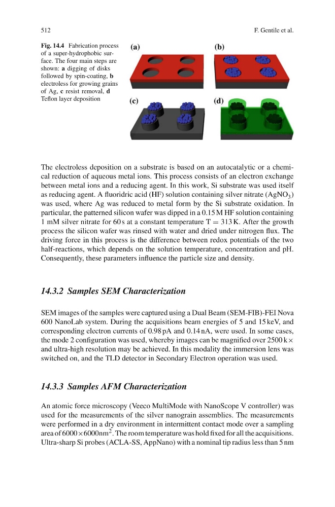
Fig. 14.4 Fabrication process
of a super-hydrophobic surface. The four main steps are
shown: a digging of disks
followed by spin-coating, b
electroless for growing grains
of Ag, c resist removal, d
Teflon layer deposition
The electroless deposition on a substrate is based on an autocatalytic or a chemical reduction of aqueous metal ions. This process consists of an electron exchange
between metal ions and a reducing agent. In this work, Si substrate was used itself
as reducing agent. A fluoridric acid (HF) solution containing silver nitrate (AgNO 3 )
was used, where Ag was reduced to metal form by the Si substrate oxidation. In
particular, the patterned silicon wafer was dipped in a 0.15 M HF solution containing
1 mM silver nitrate for 60 s at a constant temperature T = 313 K. After the growth
process the silicon wafer was rinsed with water and dried under nitrogen flux. The
driving force in this process is the difference between redox potentials of the two
half-reactions, which depends on the solution temperature, concentration and pH.
Consequently, these parameters influence the particle size and density.
14.3.2 Samples SEM Characterization
SEM images of the samples were captured using a Dual Beam (SEM-FIB)-FEI Nova
600 NanoLab system. During the acquisitions beam energies of 5 and 15 keV, and
corresponding electron currents of 0.98 pA and 0.14 nA, were used. In some cases,
the mode 2 configuration was used, whereby images can be magnified over 2500 k×
and ultra-high resolution may be achieved. In this modality the immersion lens was
switched on, and the TLD detector in Secondary Electron operation was used.
14.3.3 Samples AFM Characterization
An atomic force microscopy (Veeco MultiMode with NanoScope V controller) was
used for the measurements of the silver nanograin assemblies. The measurements
were performed in a dry environment in intermittent contact mode over a sampling
area of 6000×6000nm 2 . The room temperature was hold fixed for all the acquisitions.
Ultra-sharp Si probes (ACLA-SS, AppNano) with a nominal tip radius less than 5 nm
F. Gentile et al.
Fig. 14.4 Fabrication process
of a super-hydrophobic surface. The four main steps are
shown: a digging of disks
followed by spin-coating, b
electroless for growing grains
of Ag, c resist removal, d
Teflon layer deposition
The electroless deposition on a substrate is based on an autocatalytic or a chemical reduction of aqueous metal ions. This process consists of an electron exchange
between metal ions and a reducing agent. In this work, Si substrate was used itself
as reducing agent. A fluoridric acid (HF) solution containing silver nitrate (AgNO 3 )
was used, where Ag was reduced to metal form by the Si substrate oxidation. In
particular, the patterned silicon wafer was dipped in a 0.15 M HF solution containing
1 mM silver nitrate for 60 s at a constant temperature T = 313 K. After the growth
process the silicon wafer was rinsed with water and dried under nitrogen flux. The
driving force in this process is the difference between redox potentials of the two
half-reactions, which depends on the solution temperature, concentration and pH.
Consequently, these parameters influence the particle size and density.
14.3.2 Samples SEM Characterization
SEM images of the samples were captured using a Dual Beam (SEM-FIB)-FEI Nova
600 NanoLab system. During the acquisitions beam energies of 5 and 15 keV, and
corresponding electron currents of 0.98 pA and 0.14 nA, were used. In some cases,
the mode 2 configuration was used, whereby images can be magnified over 2500 k×
and ultra-high resolution may be achieved. In this modality the immersion lens was
switched on, and the TLD detector in Secondary Electron operation was used.
14.3.3 Samples AFM Characterization
An atomic force microscopy (Veeco MultiMode with NanoScope V controller) was
used for the measurements of the silver nanograin assemblies. The measurements
were performed in a dry environment in intermittent contact mode over a sampling
area of 6000×6000nm 2 . The room temperature was hold fixed for all the acquisitions.
Ultra-sharp Si probes (ACLA-SS, AppNano) with a nominal tip radius less than 5 nm