

366
L. D. Negro et al.
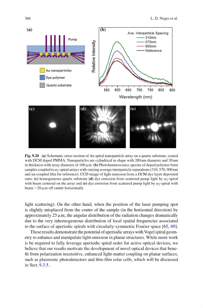
Fig. 9.20 (a) Schematic cross-section of Au spiral nanoparticle array on a quartz substrate, coated
with DCM doped PMMA. Nanoparticles are cylindrical in shape with 200 nm diameter and 30 nm
in thickness with array diameter of 100 μm. (b) Photoluminescence spectra of doped polymer form
samples coupled to γ 2 -spiral arrays with varying average interparticle separations (310, 570, 900 nm
and un-coupled film for reference). CCD image of light emission from a DCM dye layer deposited
onto: (c) homogeneous quartz substrate (d) dye emission from scattered pump light by γ 2 -spiral
with beam centered on the array and (e) dye emission from scattered pump light by γ 2 -spiral with
beam ≥20 μm off center horizontally
light scattering). On the other hand, when the position of the laser pumping spot
is slightly misplaced from the centre of the sample (in the horizontal direction) by
approximately 25 μm, the angular distribution of the radiation changes dramatically
due to the very inhomogeneous distribution of local spatial frequencies associated
to the surface of aperiodic spirals with circularly-symmetric Fourier space [65, 69].
These results demonstrate the potential of aperiodic arrays with Vogel spiral geometry to enhance and manipulate light emission in planar structures. While more work
is be required to fully leverage aperiodic spiral order for active optical devices, we
believe that our results motivate the development of novel optical devices that benefit from polarization insensitive, enhanced light-matter coupling on planar surfaces,
such as plasmonic photodetectors and thin-film solar cells, which will be discussed
in Sect. 9.3.5 .
L. D. Negro et al.
Fig. 9.20 (a) Schematic cross-section of Au spiral nanoparticle array on a quartz substrate, coated
with DCM doped PMMA. Nanoparticles are cylindrical in shape with 200 nm diameter and 30 nm
in thickness with array diameter of 100 μm. (b) Photoluminescence spectra of doped polymer form
samples coupled to γ 2 -spiral arrays with varying average interparticle separations (310, 570, 900 nm
and un-coupled film for reference). CCD image of light emission from a DCM dye layer deposited
onto: (c) homogeneous quartz substrate (d) dye emission from scattered pump light by γ 2 -spiral
with beam centered on the array and (e) dye emission from scattered pump light by γ 2 -spiral with
beam ≥20 μm off center horizontally
light scattering). On the other hand, when the position of the laser pumping spot
is slightly misplaced from the centre of the sample (in the horizontal direction) by
approximately 25 μm, the angular distribution of the radiation changes dramatically
due to the very inhomogeneous distribution of local spatial frequencies associated
to the surface of aperiodic spirals with circularly-symmetric Fourier space [65, 69].
These results demonstrate the potential of aperiodic arrays with Vogel spiral geometry to enhance and manipulate light emission in planar structures. While more work
is be required to fully leverage aperiodic spiral order for active optical devices, we
believe that our results motivate the development of novel optical devices that benefit from polarization insensitive, enhanced light-matter coupling on planar surfaces,
such as plasmonic photodetectors and thin-film solar cells, which will be discussed
in Sect. 9.3.5 .