

9 Aperiodic Order in Nanoplasmonics
349
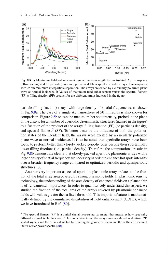
Fig. 9.8 a Maximum field enhancement versus the wavelength for an isolated Ag nanosphere
(50 nm radius) and for periodic, coprime, prime, and Ulam spiral aperiodic arrays of nanospheres
with 25 nm minimum interparticle separation. The arrays are exited by a circularly polarized plane
wave at normal incidence. b Values of maximum filed enhancement versus the spectral flatness
(SF) × filling fraction (FF) product for the different arrays indicated in the figure
particle filling fraction) arrays with large density of spatial frequencies, as shown
in Fig. 9.8a. The case of a single Ag nanosphere of 50 nm radius is also shown for
comparison. Figure 9.8b shows the maximum hot spot intensity, probed in the plane
of the arrays, for a number of aperiodic deterministic structures (named in the figure)
as a function of the product of the arrays filling fraction (FF) (or particles density)
and spectral flatness 5 (SF). To better describe the influence of both the polarization states of the incident field, the arrays were excited by a circularly polarized
plane wave at normal incidence. It is to be noted that aperiodic arrays have been
found to perform better than closely packed periodic ones despite their substantially
lower filling fractions (i.e., particle density). Therefore, the computational results in
Fig. 9.8b demonstrate clearly that closely-packed aperiodic plasmonic arrays with a
large density of spatial frequency are necessary in order to enhance hot spots intensity
over a broader frequency range compared to optimized periodic and quasiperiodic
structures [80].
Another very important aspect of aperiodic plasmonic arrays relates to the fraction of the total array area covered by strong plasmonic fields. In plasmonic sensing
technology, the understanding of the area density of enhanced fields on a planar chip
is of fundamental importance. In order to quantitatively understand this aspect, we
studied the fraction of the total area of the arrays covered by plasmonic enhanced
fields with values greater then a fixed threshold. This important feature is mathematically defined by the cumulative distribution of field enhancement (CDFE), which
we have introduced in Ref. [80].
5 The spectral flatness (SF) is a digital signal processing parameter that measures how spectrally
diffused a signal is. In the case of plasmonic structures, the arrays are considered as digitized 2D
spatial signals and the SF is calculated by dividing the geometric mean and the arithmetic mean of
their Fourier power spectra [80].
349
Fig. 9.8 a Maximum field enhancement versus the wavelength for an isolated Ag nanosphere
(50 nm radius) and for periodic, coprime, prime, and Ulam spiral aperiodic arrays of nanospheres
with 25 nm minimum interparticle separation. The arrays are exited by a circularly polarized plane
wave at normal incidence. b Values of maximum filed enhancement versus the spectral flatness
(SF) × filling fraction (FF) product for the different arrays indicated in the figure
particle filling fraction) arrays with large density of spatial frequencies, as shown
in Fig. 9.8a. The case of a single Ag nanosphere of 50 nm radius is also shown for
comparison. Figure 9.8b shows the maximum hot spot intensity, probed in the plane
of the arrays, for a number of aperiodic deterministic structures (named in the figure)
as a function of the product of the arrays filling fraction (FF) (or particles density)
and spectral flatness 5 (SF). To better describe the influence of both the polarization states of the incident field, the arrays were excited by a circularly polarized
plane wave at normal incidence. It is to be noted that aperiodic arrays have been
found to perform better than closely packed periodic ones despite their substantially
lower filling fractions (i.e., particle density). Therefore, the computational results in
Fig. 9.8b demonstrate clearly that closely-packed aperiodic plasmonic arrays with a
large density of spatial frequency are necessary in order to enhance hot spots intensity
over a broader frequency range compared to optimized periodic and quasiperiodic
structures [80].
Another very important aspect of aperiodic plasmonic arrays relates to the fraction of the total array area covered by strong plasmonic fields. In plasmonic sensing
technology, the understanding of the area density of enhanced fields on a planar chip
is of fundamental importance. In order to quantitatively understand this aspect, we
studied the fraction of the total area of the arrays covered by plasmonic enhanced
fields with values greater then a fixed threshold. This important feature is mathematically defined by the cumulative distribution of field enhancement (CDFE), which
we have introduced in Ref. [80].
5 The spectral flatness (SF) is a digital signal processing parameter that measures how spectrally
diffused a signal is. In the case of plasmonic structures, the arrays are considered as digitized 2D
spatial signals and the SF is calculated by dividing the geometric mean and the arithmetic mean of
their Fourier power spectra [80].