

190
F. Vallée and N. Del Fatti
-10
-5
0
5
T/T (x 10
-3
)
0.0
0.2
0.4
0.6
0.8
1.0
T
R
T, R
1.5
2.0
2.5
3.0
-0.15
-0.10
-0.05
0.00
0.05
0.10
t 2
r 1
t 1
r 2
(eV)
t
1,2
, r
1,2
1.5
2.0
2.5
3.0
-5
0
5
10
15
(eV)
R/R (x 10
-3
)
Δ
Δ
ω
ω
(a)
(b)
(c)
(d)
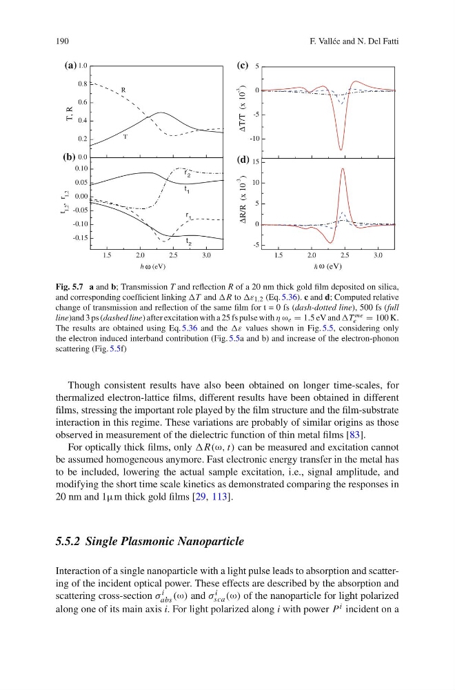
Fig. 5.7 a and b; Transmission T and reflection R of a 20 nm thick gold film deposited on silica,
and corresponding coefficient linking ωT and ωR to ωε 1,2 (Eq. 5.36). c and d; Computed relative
change of transmission and reflection of the same film for t = 0 fs (dash-dotted line), 500 fs (full
line)and 3 ps (dashed line) after excitation with a 25 fs pulse with Φ ω e = 1.5 eV and ωT me
e = 100 K.
The results are obtained using Eq. 5.36 and the ωε values shown in Fig. 5.5, considering only
the electron induced interband contribution (Fig. 5.5a and b) and increase of the electron-phonon
scattering (Fig. 5.5f)
Though consistent results have also been obtained on longer time-scales, for
thermalized electron-lattice films, different results have been obtained in different
films, stressing the important role played by the film structure and the film-substrate
interaction in this regime. These variations are probably of similar origins as those
observed in measurement of the dielectric function of thin metal films [83].
For optically thick films, only ωR(ω, t) can be measured and excitation cannot
be assumed homogeneous anymore. Fast electronic energy transfer in the metal has
to be included, lowering the actual sample excitation, i.e., signal amplitude, and
modifying the short time scale kinetics as demonstrated comparing the responses in
20 nm and 1μm thick gold films [29, 113].
5.5.2 Single Plasmonic Nanoparticle
Interaction of a single nanoparticle with a light pulse leads to absorption and scattering of the incident optical power. These effects are described by the absorption and
scattering cross-section η i
abs (ω) and η i
sca (ω) of the nanoparticle for light polarized
along one of its main axis i. For light polarized along i with power P i incident on a
F. Vallée and N. Del Fatti
-10
-5
0
5
T/T (x 10
-3
)
0.0
0.2
0.4
0.6
0.8
1.0
T
R
T, R
1.5
2.0
2.5
3.0
-0.15
-0.10
-0.05
0.00
0.05
0.10
t 2
r 1
t 1
r 2
(eV)
t
1,2
, r
1,2
1.5
2.0
2.5
3.0
-5
0
5
10
15
(eV)
R/R (x 10
-3
)
Δ
Δ
ω
ω
(a)
(b)
(c)
(d)
Fig. 5.7 a and b; Transmission T and reflection R of a 20 nm thick gold film deposited on silica,
and corresponding coefficient linking ωT and ωR to ωε 1,2 (Eq. 5.36). c and d; Computed relative
change of transmission and reflection of the same film for t = 0 fs (dash-dotted line), 500 fs (full
line)and 3 ps (dashed line) after excitation with a 25 fs pulse with Φ ω e = 1.5 eV and ωT me
e = 100 K.
The results are obtained using Eq. 5.36 and the ωε values shown in Fig. 5.5, considering only
the electron induced interband contribution (Fig. 5.5a and b) and increase of the electron-phonon
scattering (Fig. 5.5f)
Though consistent results have also been obtained on longer time-scales, for
thermalized electron-lattice films, different results have been obtained in different
films, stressing the important role played by the film structure and the film-substrate
interaction in this regime. These variations are probably of similar origins as those
observed in measurement of the dielectric function of thin metal films [83].
For optically thick films, only ωR(ω, t) can be measured and excitation cannot
be assumed homogeneous anymore. Fast electronic energy transfer in the metal has
to be included, lowering the actual sample excitation, i.e., signal amplitude, and
modifying the short time scale kinetics as demonstrated comparing the responses in
20 nm and 1μm thick gold films [29, 113].
5.5.2 Single Plasmonic Nanoparticle
Interaction of a single nanoparticle with a light pulse leads to absorption and scattering of the incident optical power. These effects are described by the absorption and
scattering cross-section η i
abs (ω) and η i
sca (ω) of the nanoparticle for light polarized
along one of its main axis i. For light polarized along i with power P i incident on a