

(Fig. 3b). After the set operation, the dark region is observed between the two
electrodes. Element analysis shows that the dark region is composed of Cu
[9]. The thickness of the Cu filament is around 30 nm. The thickness depends on
the on the conductance of the switch, which is controlled by the current during set
operation. Here we intentionally form a thick filament for observation and the on
resistance is a several tens ohm. This experiment shows that the low conductance is
originated from the Cu filament in the solid electrolyte.
To apply the atomic switch to the programmable switch in FPGA, a high off-state
reliability is required. During a logic operation, a constant operation voltage (V DD ) is
applied to the off-state switch. Thus, the switch needs to persist its off state for ten
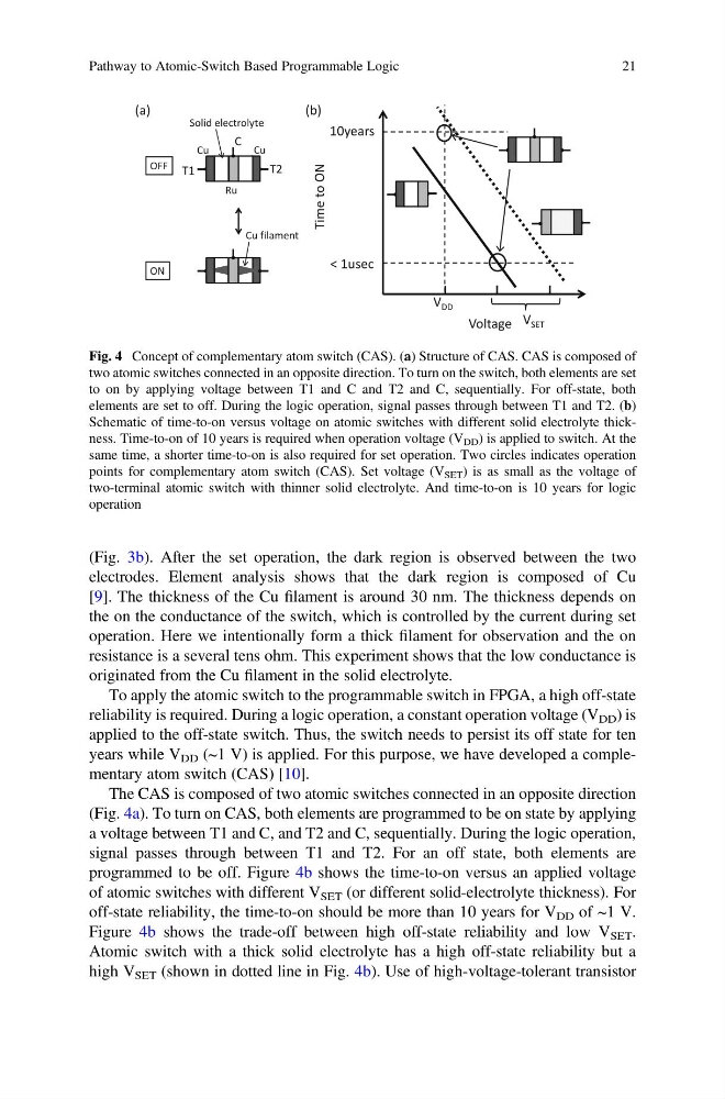
years while V DD (~1 V) is applied. For this purpose, we have developed a complementary atom switch (CAS) [10].
The CAS is composed of two atomic switches connected in an opposite direction
(Fig. 4a). To turn on CAS, both elements are programmed to be on state by applying
a voltage between T1 and C, and T2 and C, sequentially. During the logic operation,
signal passes through between T1 and T2. For an off state, both elements are
programmed to be off. Figure 4b shows the time-to-on versus an applied voltage
of atomic switches with different V SET (or different solid-electrolyte thickness). For
off-state reliability, the time-to-on should be more than 10 years for V DD of ~1 V.
Figure 4b shows the trade-off between high off-state reliability and low V SET .
Atomic switch with a thick solid electrolyte has a high off-state reliability but a
high V SET (shown in dotted line in Fig. 4b). Use of high-voltage-tolerant transistor
T1
T2
Time to ON
Voltage
< 1usec
10years
V SET
V DD
ON
Cu
Solid electrolyte
Ru
OFF
Cu
C
(a)
(b)
Cu filament
Fig. 4 Concept of complementary atom switch (CAS). (a) Structure of CAS. CAS is composed of
two atomic switches connected in an opposite direction. To turn on the switch, both elements are set
to on by applying voltage between T1 and C and T2 and C, sequentially. For off-state, both
elements are set to off. During the logic operation, signal passes through between T1 and T2. (b)
Schematic of time-to-on versus voltage on atomic switches with different solid electrolyte thickness. Time-to-on of 10 years is required when operation voltage (V DD ) is applied to switch. At the
same time, a shorter time-to-on is also required for set operation. Two circles indicates operation
points for complementary atom switch (CAS). Set voltage (V SET ) is as small as the voltage of
two-terminal atomic switch with thinner solid electrolyte. And time-to-on is 10 years for logic
operation
Pathway to Atomic-Switch Based Programmable Logic
21
electrodes. Element analysis shows that the dark region is composed of Cu
[9]. The thickness of the Cu filament is around 30 nm. The thickness depends on
the on the conductance of the switch, which is controlled by the current during set
operation. Here we intentionally form a thick filament for observation and the on
resistance is a several tens ohm. This experiment shows that the low conductance is
originated from the Cu filament in the solid electrolyte.
To apply the atomic switch to the programmable switch in FPGA, a high off-state
reliability is required. During a logic operation, a constant operation voltage (V DD ) is
applied to the off-state switch. Thus, the switch needs to persist its off state for ten
years while V DD (~1 V) is applied. For this purpose, we have developed a complementary atom switch (CAS) [10].
The CAS is composed of two atomic switches connected in an opposite direction
(Fig. 4a). To turn on CAS, both elements are programmed to be on state by applying
a voltage between T1 and C, and T2 and C, sequentially. During the logic operation,
signal passes through between T1 and T2. For an off state, both elements are
programmed to be off. Figure 4b shows the time-to-on versus an applied voltage
of atomic switches with different V SET (or different solid-electrolyte thickness). For
off-state reliability, the time-to-on should be more than 10 years for V DD of ~1 V.
Figure 4b shows the trade-off between high off-state reliability and low V SET .
Atomic switch with a thick solid electrolyte has a high off-state reliability but a
high V SET (shown in dotted line in Fig. 4b). Use of high-voltage-tolerant transistor
T1
T2
Time to ON
Voltage
< 1usec
10years
V SET
V DD
ON
Cu
Solid electrolyte
Ru
OFF
Cu
C
(a)
(b)
Cu filament
Fig. 4 Concept of complementary atom switch (CAS). (a) Structure of CAS. CAS is composed of
two atomic switches connected in an opposite direction. To turn on the switch, both elements are set
to on by applying voltage between T1 and C and T2 and C, sequentially. For off-state, both
elements are set to off. During the logic operation, signal passes through between T1 and T2. (b)
Schematic of time-to-on versus voltage on atomic switches with different solid electrolyte thickness. Time-to-on of 10 years is required when operation voltage (V DD ) is applied to switch. At the
same time, a shorter time-to-on is also required for set operation. Two circles indicates operation
points for complementary atom switch (CAS). Set voltage (V SET ) is as small as the voltage of
two-terminal atomic switch with thinner solid electrolyte. And time-to-on is 10 years for logic
operation
Pathway to Atomic-Switch Based Programmable Logic
21