

5 Results: Atomic Switch Network Dynamics
5.1 Operational Characteristics of the Atomic Switch
Experimental studies into the operational characteristics of atomic switches has
recently promulgated attention from the perspective of modeling and simulation.
Atomic switches are known to operate through two mechanisms: (1) formation/
dissolution of conductive filaments, and (2) a phase transition between monoclinic
acanthite (α) and body centered cubic argentite (β) within Ag 2 S. Application of a bias
voltage across the junction has been shown using transmission electron microscopy
to induce the formation of nanoscale conducting channels across the Ag 2 S interface
through a bias-catalyzed phase transition, converting the surrounding α-Ag 2 S matrix
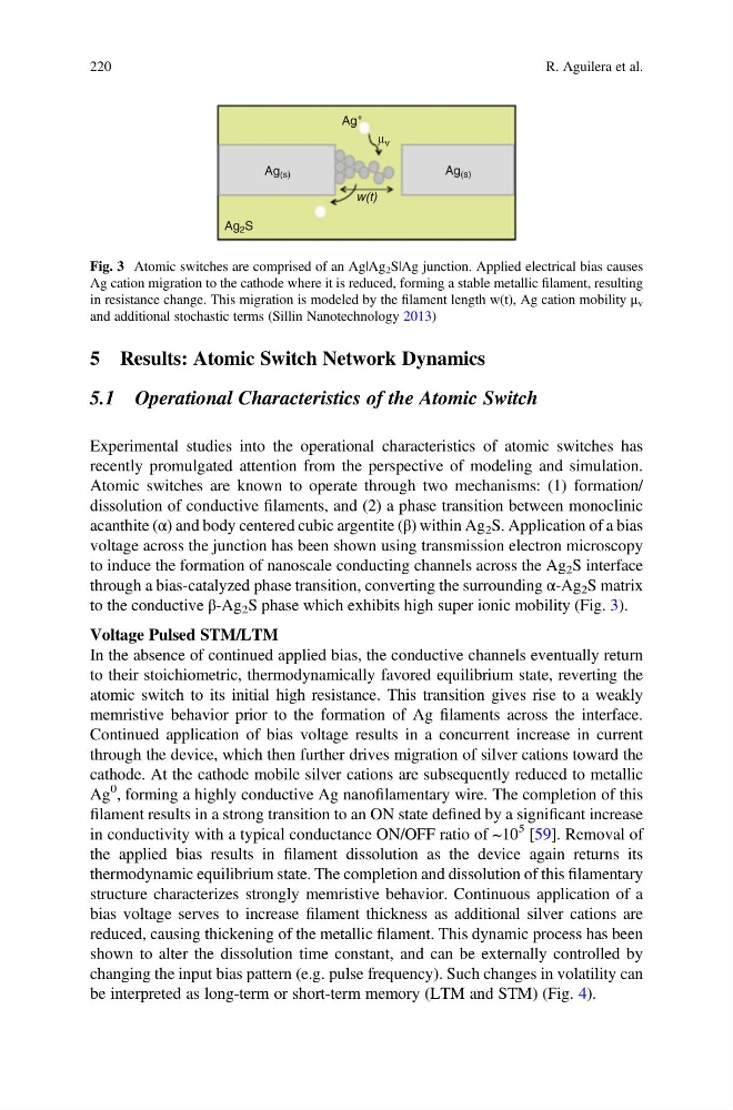
to the conductive β-Ag 2 S phase which exhibits high super ionic mobility (Fig. 3).
Voltage Pulsed STM/LTM
In the absence of continued applied bias, the conductive channels eventually return
to their stoichiometric, thermodynamically favored equilibrium state, reverting the
atomic switch to its initial high resistance. This transition gives rise to a weakly
memristive behavior prior to the formation of Ag filaments across the interface.
Continued application of bias voltage results in a concurrent increase in current
through the device, which then further drives migration of silver cations toward the
cathode. At the cathode mobile silver cations are subsequently reduced to metallic
Ag
0 , forming a highly conductive Ag nanofilamentary wire. The completion of this
filament results in a strong transition to an ON state defined by a significant increase
in conductivity with a typical conductance ON/OFF ratio of ~10
5 [59]. Removal of
the applied bias results in filament dissolution as the device again returns its
thermodynamic equilibrium state. The completion and dissolution of this filamentary
structure characterizes strongly memristive behavior. Continuous application of a
bias voltage serves to increase filament thickness as additional silver cations are
reduced, causing thickening of the metallic filament. This dynamic process has been
shown to alter the dissolution time constant, and can be externally controlled by
changing the input bias pattern (e.g. pulse frequency). Such changes in volatility can
be interpreted as long-term or short-term memory (LTM and STM) (Fig. 4).
Ag
+
Ag 2 S
Ag (s)
Ag (s)
µ v
w(t)
Fig. 3 Atomic switches are comprised of an Ag|Ag 2 S|Ag junction. Applied electrical bias causes
Ag cation migration to the cathode where it is reduced, forming a stable metallic filament, resulting
in resistance change. This migration is modeled by the filament length w(t), Ag cation mobility μ v
and additional stochastic terms (Sillin Nanotechnology 2013)
220
R. Aguilera et al.
5.1 Operational Characteristics of the Atomic Switch
Experimental studies into the operational characteristics of atomic switches has
recently promulgated attention from the perspective of modeling and simulation.
Atomic switches are known to operate through two mechanisms: (1) formation/
dissolution of conductive filaments, and (2) a phase transition between monoclinic
acanthite (α) and body centered cubic argentite (β) within Ag 2 S. Application of a bias
voltage across the junction has been shown using transmission electron microscopy
to induce the formation of nanoscale conducting channels across the Ag 2 S interface
through a bias-catalyzed phase transition, converting the surrounding α-Ag 2 S matrix
to the conductive β-Ag 2 S phase which exhibits high super ionic mobility (Fig. 3).
Voltage Pulsed STM/LTM
In the absence of continued applied bias, the conductive channels eventually return
to their stoichiometric, thermodynamically favored equilibrium state, reverting the
atomic switch to its initial high resistance. This transition gives rise to a weakly
memristive behavior prior to the formation of Ag filaments across the interface.
Continued application of bias voltage results in a concurrent increase in current
through the device, which then further drives migration of silver cations toward the
cathode. At the cathode mobile silver cations are subsequently reduced to metallic
Ag
0 , forming a highly conductive Ag nanofilamentary wire. The completion of this
filament results in a strong transition to an ON state defined by a significant increase
in conductivity with a typical conductance ON/OFF ratio of ~10
5 [59]. Removal of
the applied bias results in filament dissolution as the device again returns its
thermodynamic equilibrium state. The completion and dissolution of this filamentary
structure characterizes strongly memristive behavior. Continuous application of a
bias voltage serves to increase filament thickness as additional silver cations are
reduced, causing thickening of the metallic filament. This dynamic process has been
shown to alter the dissolution time constant, and can be externally controlled by
changing the input bias pattern (e.g. pulse frequency). Such changes in volatility can
be interpreted as long-term or short-term memory (LTM and STM) (Fig. 4).
Ag
+
Ag 2 S
Ag (s)
Ag (s)
µ v
w(t)
Fig. 3 Atomic switches are comprised of an Ag|Ag 2 S|Ag junction. Applied electrical bias causes
Ag cation migration to the cathode where it is reduced, forming a stable metallic filament, resulting
in resistance change. This migration is modeled by the filament length w(t), Ag cation mobility μ v
and additional stochastic terms (Sillin Nanotechnology 2013)
220
R. Aguilera et al.