

spontaneously formed a complex network. Again, network density exhibited
non-uniformity due to the stochasticity associated with drop casting metal
suspensions.
Successful implementations of the ELD reaction above allowed us to design a
technique using highly patterned top-down photolithography combined with complex spontaneous and self-organized growth. The patterned seed networks consist of
a 2 μm layer of AZ nLOF 2020 (a negative photoresist), a soft bake, followed by UV
photolithography, and a post-exposure bake. This resist is developed in MF26A,
rinsed with isopropanol, and a 300 nm layer of copper is then deposited and lifted off
overnight in acetone. At the end of this process, a patterned grid of copper posts
300 nm high is left. The size and pitch of these posts were refined over time to give
the most desirable silver crystal growth [59].
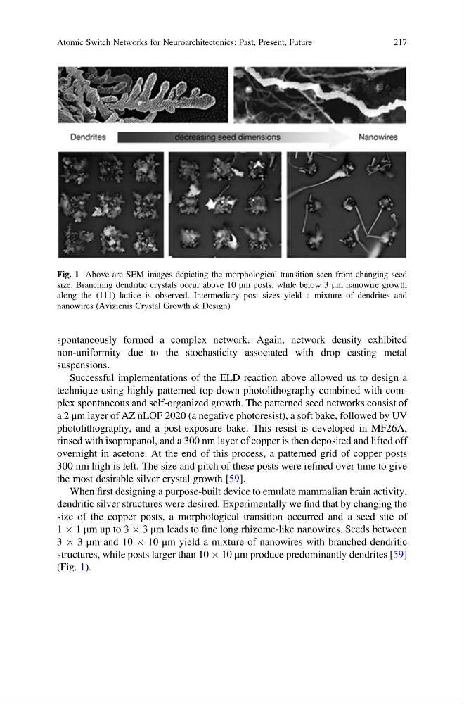
When first designing a purpose-built device to emulate mammalian brain activity,
dendritic silver structures were desired. Experimentally we find that by changing the
size of the copper posts, a morphological transition occurred and a seed site of
1 Â 1 μm up to 3 Â 3 μm leads to fine long rhizome-like nanowires. Seeds between
3 Â 3 μm and 10 Â 10 μm yield a mixture of nanowires with branched dendritic
structures, while posts larger than 10 Â 10 μm produce predominantly dendrites [59]
(Fig. 1).
Fig. 1 Above are SEM images depicting the morphological transition seen from changing seed
size. Branching dendritic crystals occur above 10 μm posts, while below 3 μm nanowire growth
along the (111) lattice is observed. Intermediary post sizes yield a mixture of dendrites and
nanowires (Avizienis Crystal Growth & Design)
Atomic Switch Networks for Neuroarchitectonics: Past, Present, Future
217
non-uniformity due to the stochasticity associated with drop casting metal
suspensions.
Successful implementations of the ELD reaction above allowed us to design a
technique using highly patterned top-down photolithography combined with complex spontaneous and self-organized growth. The patterned seed networks consist of
a 2 μm layer of AZ nLOF 2020 (a negative photoresist), a soft bake, followed by UV
photolithography, and a post-exposure bake. This resist is developed in MF26A,
rinsed with isopropanol, and a 300 nm layer of copper is then deposited and lifted off
overnight in acetone. At the end of this process, a patterned grid of copper posts
300 nm high is left. The size and pitch of these posts were refined over time to give
the most desirable silver crystal growth [59].
When first designing a purpose-built device to emulate mammalian brain activity,
dendritic silver structures were desired. Experimentally we find that by changing the
size of the copper posts, a morphological transition occurred and a seed site of
1 Â 1 μm up to 3 Â 3 μm leads to fine long rhizome-like nanowires. Seeds between
3 Â 3 μm and 10 Â 10 μm yield a mixture of nanowires with branched dendritic
structures, while posts larger than 10 Â 10 μm produce predominantly dendrites [59]
(Fig. 1).
Fig. 1 Above are SEM images depicting the morphological transition seen from changing seed
size. Branching dendritic crystals occur above 10 μm posts, while below 3 μm nanowire growth
along the (111) lattice is observed. Intermediary post sizes yield a mixture of dendrites and
nanowires (Avizienis Crystal Growth & Design)
Atomic Switch Networks for Neuroarchitectonics: Past, Present, Future
217