

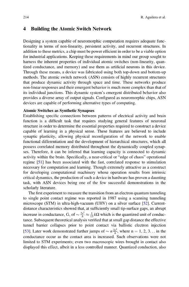
4 Building the Atomic Switch Network
Designing a system capable of neuromorphic computation requires adequate functionality in terms of non-linearity, persistent activity, and recurrent structures. In
addition to these metrics, a chip must be power efficient in order to be a viable option
for industrial applications. Keeping these requirements in mind our group sought to
harness the inherent properties of individual atomic switches (non-linearity, quantized conductance, and memory) and use them as artificial neurons in this device.
Through these means, a device was fabricated using both top-down and bottom-up
methods. The atomic switch network (ASN) consists of highly recurrent structures
that produce dynamic activity through space and time. These networks produce
non-linear responses and their emergent behavior is much more complex than that of
its individual junctions. This dynamic system’s emergent distributed behavior also
provides a diverse array of output signals. Configured as neuromorphic chips, ASN
devices are capable of performing alternative types of computing.
Atomic Switches as Synthetic Synapses
Establishing specific connections between patterns of electrical activity and brain
function is a difficult task that requires studying general features of neuronal
structure in order to determine the essential properties required to construct a device
capable of learning in a physical sense. These features are believed to include
synaptic plasticity, allowing physical reconfiguration of the network to enable
functional differentiation and the development of hierarchical structures, which all
possess correlated memory distributed throughout the dynamically coupled synapses. Therefore, it can be inferred that learning capacity is connected to dynamic
activity within the brain. Specifically, a near-critical or “edge of chaos” operational
regime [51] has been associated with the fast, correlated response to stimulation
necessary for computation and learning. Though extremely attractive as a construct
for developing computational machinery whose operation results from intrinsic
critical dynamics, the production of such a device in hardware has proven a daunting
task, with ASN devices being one of the few successful demonstrations in the
scholarly literature.
The first experiment to measure the transition from an electron quantum tunneling
to single point contact regime was reported in 1987 using a scanning tunneling
microscope (STM) in ultra-high-vacuum (UHV) on a silver surface [52]. Currentdistance characteristics showed that, at sufficiently small tip-surface gaps, an abrupt
increase in conductance, G, of $
2e
2
h %
1
13 kΩ which is the quantized unit of conductance. Subsequent theoretical analysis verified that at small gap distance the effective
tunnel barrier collapses prior to point contact via ballistic electron injection
[53]. Later work demonstrated further jumps of $ n
2e
2
h , where n ¼ 1, 2, 3. . . in the
conductance occur as the contact area is increased. Such observations were not
limited to STM experiments; even two macroscopic wires brought in contact also
displayed this effect, albeit in a less controlled manner. Quantized conduction, also
214
R. Aguilera et al.
Designing a system capable of neuromorphic computation requires adequate functionality in terms of non-linearity, persistent activity, and recurrent structures. In
addition to these metrics, a chip must be power efficient in order to be a viable option
for industrial applications. Keeping these requirements in mind our group sought to
harness the inherent properties of individual atomic switches (non-linearity, quantized conductance, and memory) and use them as artificial neurons in this device.
Through these means, a device was fabricated using both top-down and bottom-up
methods. The atomic switch network (ASN) consists of highly recurrent structures
that produce dynamic activity through space and time. These networks produce
non-linear responses and their emergent behavior is much more complex than that of
its individual junctions. This dynamic system’s emergent distributed behavior also
provides a diverse array of output signals. Configured as neuromorphic chips, ASN
devices are capable of performing alternative types of computing.
Atomic Switches as Synthetic Synapses
Establishing specific connections between patterns of electrical activity and brain
function is a difficult task that requires studying general features of neuronal
structure in order to determine the essential properties required to construct a device
capable of learning in a physical sense. These features are believed to include
synaptic plasticity, allowing physical reconfiguration of the network to enable
functional differentiation and the development of hierarchical structures, which all
possess correlated memory distributed throughout the dynamically coupled synapses. Therefore, it can be inferred that learning capacity is connected to dynamic
activity within the brain. Specifically, a near-critical or “edge of chaos” operational
regime [51] has been associated with the fast, correlated response to stimulation
necessary for computation and learning. Though extremely attractive as a construct
for developing computational machinery whose operation results from intrinsic
critical dynamics, the production of such a device in hardware has proven a daunting
task, with ASN devices being one of the few successful demonstrations in the
scholarly literature.
The first experiment to measure the transition from an electron quantum tunneling
to single point contact regime was reported in 1987 using a scanning tunneling
microscope (STM) in ultra-high-vacuum (UHV) on a silver surface [52]. Currentdistance characteristics showed that, at sufficiently small tip-surface gaps, an abrupt
increase in conductance, G, of $
2e
2
h %
1
13 kΩ which is the quantized unit of conductance. Subsequent theoretical analysis verified that at small gap distance the effective
tunnel barrier collapses prior to point contact via ballistic electron injection
[53]. Later work demonstrated further jumps of $ n
2e
2
h , where n ¼ 1, 2, 3. . . in the
conductance occur as the contact area is increased. Such observations were not
limited to STM experiments; even two macroscopic wires brought in contact also
displayed this effect, albeit in a less controlled manner. Quantized conduction, also
214
R. Aguilera et al.