

1 (V 1 ) or input 2 (V 2 ), and the value of 0 indicates a state where no voltage is applied
to them. Depending on the voltage application conditions of input 1 and input
2, bridges of the Ag filaments between the Ag/Ag 2 S wire and the Pt wires form or
disappear at each atomic switch. For instance, an AND gate was consisted of two
atomic switches with one Ag/Ag 2 S wire and two Pt wires (see Fig. 9a). The output
voltage (V out ) was detected only when voltages are applied to both input 1 and input
2. Also, in an OR gate consisted of two atomic switches with two Ag/Ag 2 S wires and
one Pt wire, no voltage of V out was detected only when no voltage was applied to
either of the two inputs of 1 and 2 (see Fig. 9b). In the NOT gate consisted of one
atomic switch with one Ag/Ag 2 S wire and one Pt wire, the output voltage of V out
was detected only when no voltage was applied to the input 1 (see Fig. 9c). By
combining these basic logic gates of the AND gate, the OR gate and the NOT gate, it
is possible to construct logic circuits for the computer.
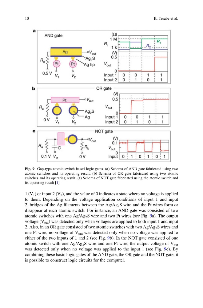
Fig. 9 Gap-type atomic switch based logic gates. (a) Schema of AND gate fabricated using two
atomic switches and its operating result. (b) Schema of OR gate fabricated using two atomic
switches and its operating result. (c) Schema of NOT gate fabricated using the atomic switch and
its operating result [1]
10
K. Terabe et al.
to them. Depending on the voltage application conditions of input 1 and input
2, bridges of the Ag filaments between the Ag/Ag 2 S wire and the Pt wires form or
disappear at each atomic switch. For instance, an AND gate was consisted of two
atomic switches with one Ag/Ag 2 S wire and two Pt wires (see Fig. 9a). The output
voltage (V out ) was detected only when voltages are applied to both input 1 and input
2. Also, in an OR gate consisted of two atomic switches with two Ag/Ag 2 S wires and
one Pt wire, no voltage of V out was detected only when no voltage was applied to
either of the two inputs of 1 and 2 (see Fig. 9b). In the NOT gate consisted of one
atomic switch with one Ag/Ag 2 S wire and one Pt wire, the output voltage of V out
was detected only when no voltage was applied to the input 1 (see Fig. 9c). By
combining these basic logic gates of the AND gate, the OR gate and the NOT gate, it
is possible to construct logic circuits for the computer.
Fig. 9 Gap-type atomic switch based logic gates. (a) Schema of AND gate fabricated using two
atomic switches and its operating result. (b) Schema of OR gate fabricated using two atomic
switches and its operating result. (c) Schema of NOT gate fabricated using the atomic switch and
its operating result [1]
10
K. Terabe et al.