

reduction and oxidation (redox) reaction or (2) electrostatic carrier doping using
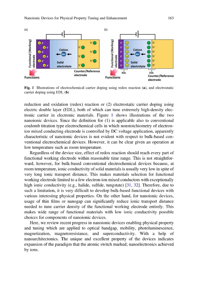
electric double layer (EDL), both of which can tune extremely high-density electronic carrier in electronic materials. Figure 1 shows illustrations of the two
nanoionic devices. Since the definition for (1) is applicable also to conventional
coulomb titration type electrochemical cells in which nonstoichiometry of electronion mixed conducting electrode is controlled by DC voltage application, apparently
characteristic of nanoionic devices is not evident with respect to bulk-based conventional electrochemical devices. However, it can be clear given an operation at
low temperature such as room temperature.
Regardless of the device size, effect of redox reaction should reach every part of
functional working electrode within reasonable time range. This is not straightforward, however, for bulk-based conventional electrochemical devices because, at
room temperature, ionic conductivity of solid materials is usually very low in spite of
very long ionic transport distance. This makes materials selection for functional
working electrode limited to a few electron-ion mixed conductors with exceptionally
high ionic conductivity (e.g., halide, sulfide, tungstate) [31, 32]. Therefore, due to
such a limitation, it is very difficult to develop bulk-based functional devices with
various interesting physical properties. On the other hand, for nanoionic devices,
usage of thin films or nanogap can significantly reduce ionic transport distance
needed to tune carrier density of the functional working electrode entirely. This
makes wide range of functional materials with low ionic conductivity possible
choices for components of nanoionic devices.
Here, we review recent progress in nanoionic devices enabling physical property
and tuning which are applied to optical bandgap, mobility, photoluminescence,
magnetization, magnetoresistance, and superconductivity. With a help of
nanoarchitectonics. The unique and excellent property of the devices indicates
expansion of the paradigm that the atomic switch marked; nanoelectronics achieved
by ions.
Fig. 1 Illustrations of electrochemical carrier doping using redox reaction (a), and electrostatic
carrier doping using EDL (b)
Nanoionic Devices for Physical Property Tuning and Enhancement
163
electric double layer (EDL), both of which can tune extremely high-density electronic carrier in electronic materials. Figure 1 shows illustrations of the two
nanoionic devices. Since the definition for (1) is applicable also to conventional
coulomb titration type electrochemical cells in which nonstoichiometry of electronion mixed conducting electrode is controlled by DC voltage application, apparently
characteristic of nanoionic devices is not evident with respect to bulk-based conventional electrochemical devices. However, it can be clear given an operation at
low temperature such as room temperature.
Regardless of the device size, effect of redox reaction should reach every part of
functional working electrode within reasonable time range. This is not straightforward, however, for bulk-based conventional electrochemical devices because, at
room temperature, ionic conductivity of solid materials is usually very low in spite of
very long ionic transport distance. This makes materials selection for functional
working electrode limited to a few electron-ion mixed conductors with exceptionally
high ionic conductivity (e.g., halide, sulfide, tungstate) [31, 32]. Therefore, due to
such a limitation, it is very difficult to develop bulk-based functional devices with
various interesting physical properties. On the other hand, for nanoionic devices,
usage of thin films or nanogap can significantly reduce ionic transport distance
needed to tune carrier density of the functional working electrode entirely. This
makes wide range of functional materials with low ionic conductivity possible
choices for components of nanoionic devices.
Here, we review recent progress in nanoionic devices enabling physical property
and tuning which are applied to optical bandgap, mobility, photoluminescence,
magnetization, magnetoresistance, and superconductivity. With a help of
nanoarchitectonics. The unique and excellent property of the devices indicates
expansion of the paradigm that the atomic switch marked; nanoelectronics achieved
by ions.
Fig. 1 Illustrations of electrochemical carrier doping using redox reaction (a), and electrostatic
carrier doping using EDL (b)
Nanoionic Devices for Physical Property Tuning and Enhancement
163