

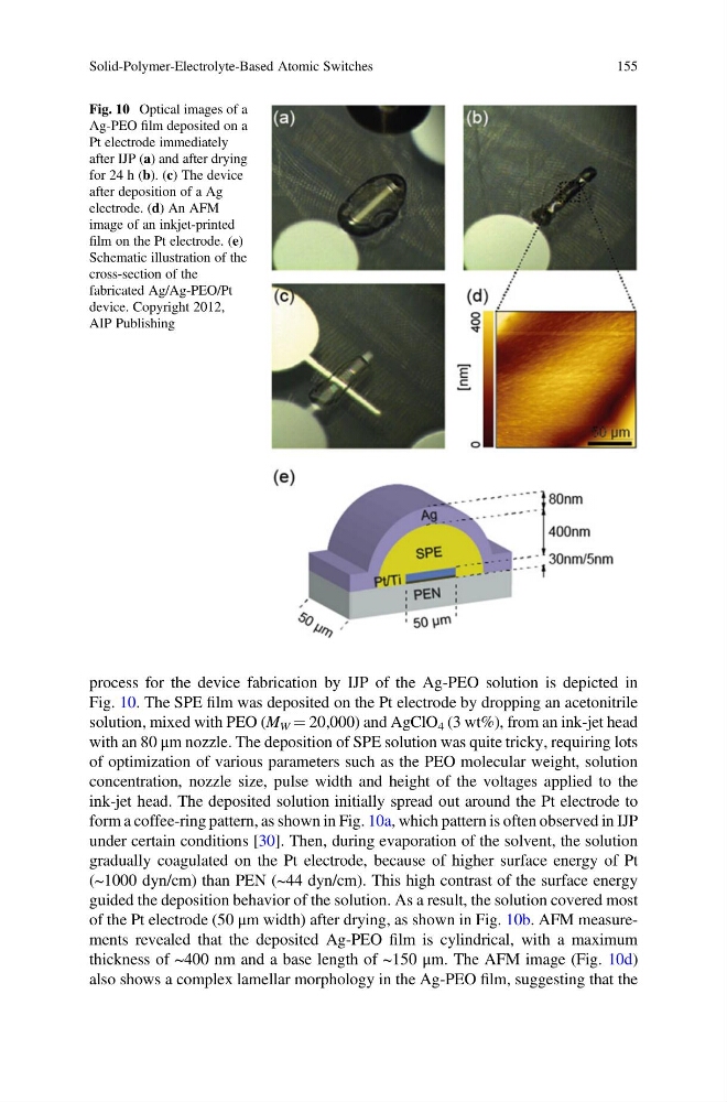
process for the device fabrication by IJP of the Ag-PEO solution is depicted in
Fig. 10. The SPE film was deposited on the Pt electrode by dropping an acetonitrile
solution, mixed with PEO (M W ¼ 20,000) and AgClO 4 (3 wt%), from an ink-jet head
with an 80 μm nozzle. The deposition of SPE solution was quite tricky, requiring lots
of optimization of various parameters such as the PEO molecular weight, solution
concentration, nozzle size, pulse width and height of the voltages applied to the
ink-jet head. The deposited solution initially spread out around the Pt electrode to
form a coffee-ring pattern, as shown in Fig. 10a, which pattern is often observed in IJP
under certain conditions [30]. Then, during evaporation of the solvent, the solution
gradually coagulated on the Pt electrode, because of higher surface energy of Pt
(~1000 dyn/cm) than PEN (~44 dyn/cm). This high contrast of the surface energy
guided the deposition behavior of the solution. As a result, the solution covered most
of the Pt electrode (50 μm width) after drying, as shown in Fig. 10b. AFM measurements revealed that the deposited Ag-PEO film is cylindrical, with a maximum
thickness of ~400 nm and a base length of ~150 μm. The AFM image (Fig. 10d)
also shows a complex lamellar morphology in the Ag-PEO film, suggesting that the
Fig. 10 Optical images of a
Ag-PEO film deposited on a
Pt electrode immediately
after IJP (a) and after drying
for 24 h (b). (c) The device
after deposition of a Ag
electrode. (d) An AFM
image of an inkjet-printed
film on the Pt electrode. (e)
Schematic illustration of the
cross-section of the
fabricated Ag/Ag-PEO/Pt
device. Copyright 2012,
AIP Publishing
Solid-Polymer-Electrolyte-Based Atomic Switches
155
Fig. 10. The SPE film was deposited on the Pt electrode by dropping an acetonitrile
solution, mixed with PEO (M W ¼ 20,000) and AgClO 4 (3 wt%), from an ink-jet head
with an 80 μm nozzle. The deposition of SPE solution was quite tricky, requiring lots
of optimization of various parameters such as the PEO molecular weight, solution
concentration, nozzle size, pulse width and height of the voltages applied to the
ink-jet head. The deposited solution initially spread out around the Pt electrode to
form a coffee-ring pattern, as shown in Fig. 10a, which pattern is often observed in IJP
under certain conditions [30]. Then, during evaporation of the solvent, the solution
gradually coagulated on the Pt electrode, because of higher surface energy of Pt
(~1000 dyn/cm) than PEN (~44 dyn/cm). This high contrast of the surface energy
guided the deposition behavior of the solution. As a result, the solution covered most
of the Pt electrode (50 μm width) after drying, as shown in Fig. 10b. AFM measurements revealed that the deposited Ag-PEO film is cylindrical, with a maximum
thickness of ~400 nm and a base length of ~150 μm. The AFM image (Fig. 10d)
also shows a complex lamellar morphology in the Ag-PEO film, suggesting that the
Fig. 10 Optical images of a
Ag-PEO film deposited on a
Pt electrode immediately
after IJP (a) and after drying
for 24 h (b). (c) The device
after deposition of a Ag
electrode. (d) An AFM
image of an inkjet-printed
film on the Pt electrode. (e)
Schematic illustration of the
cross-section of the
fabricated Ag/Ag-PEO/Pt
device. Copyright 2012,
AIP Publishing
Solid-Polymer-Electrolyte-Based Atomic Switches
155