

5 Flexible Switch/Memory Applications
The process of fabricating device components with solution drop-casting or spincoating techniques are considered to be more cost effective and easier than expensive
lithographic techniques. Specifically, for polymer materials, solution-based deposition techniques are widely accepted. However, these solution casting methods
sometimes lack the ability to control the thickness of SPE layers and pin-pointing
of the deposition area. To overcome these problems, we tried a drop-on-demand
ink-jet printing (IJP) method for deposition of SPE solutions. The advantage of IJP is
that the required amount of the target solution is deposited onto specified positions
only when needed; thus, it is more economical than other deposition methods
[27]. In this section, we present the fabrication and characterization of atomic
switches using an IJP SPE film. Most of this section is reproduced with permissions
from Ref. 28. Copyright 2012 AIP Publishing, and from Ref. 29. Copyright 2012
Cambridge University Press.
A Ag/Ag-PEO/Pt device was fabricated on a polyethylene naphthalate (PEN)
substrate with a thickness of 0.2 mm, on which 5-nm-thick Ti and 30-nm thick Pt
were formed as the adhesion layer and bottom electrode [28]. The step-by-step
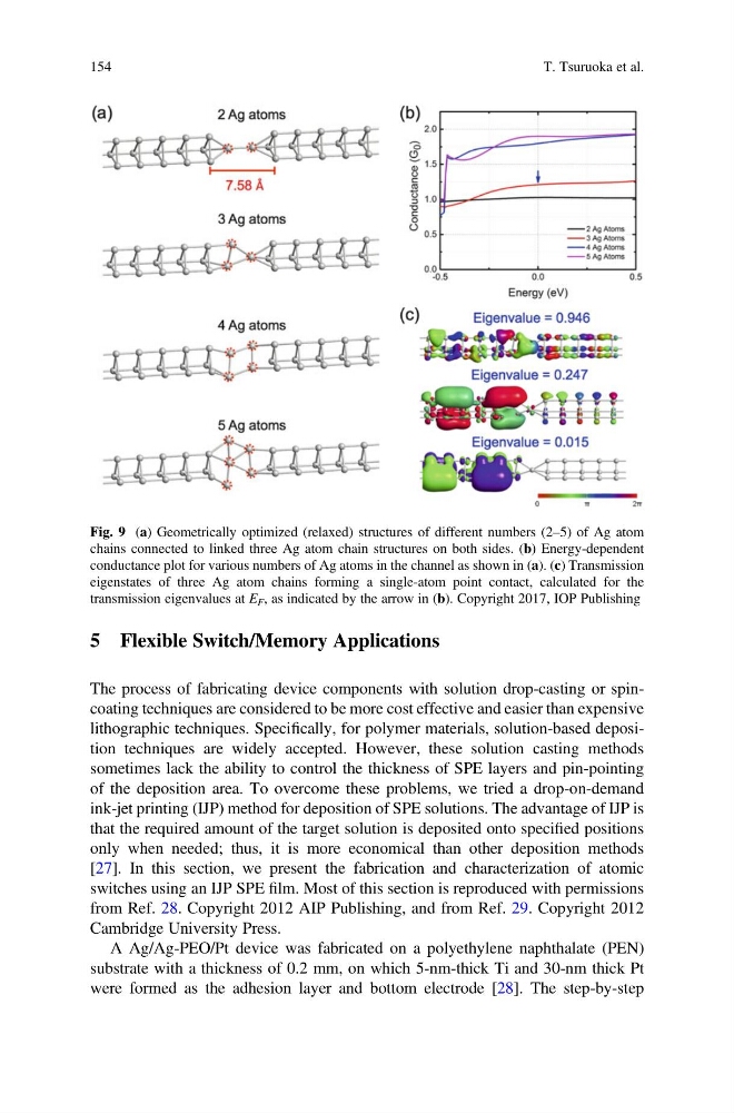
Fig. 9 (a) Geometrically optimized (relaxed) structures of different numbers (2–5) of Ag atom
chains connected to linked three Ag atom chain structures on both sides. (b) Energy-dependent
conductance plot for various numbers of Ag atoms in the channel as shown in (a). (c) Transmission
eigenstates of three Ag atom chains forming a single-atom point contact, calculated for the
transmission eigenvalues at E F , as indicated by the arrow in (b). Copyright 2017, IOP Publishing
154
T. Tsuruoka et al.
The process of fabricating device components with solution drop-casting or spincoating techniques are considered to be more cost effective and easier than expensive
lithographic techniques. Specifically, for polymer materials, solution-based deposition techniques are widely accepted. However, these solution casting methods
sometimes lack the ability to control the thickness of SPE layers and pin-pointing
of the deposition area. To overcome these problems, we tried a drop-on-demand
ink-jet printing (IJP) method for deposition of SPE solutions. The advantage of IJP is
that the required amount of the target solution is deposited onto specified positions
only when needed; thus, it is more economical than other deposition methods
[27]. In this section, we present the fabrication and characterization of atomic
switches using an IJP SPE film. Most of this section is reproduced with permissions
from Ref. 28. Copyright 2012 AIP Publishing, and from Ref. 29. Copyright 2012
Cambridge University Press.
A Ag/Ag-PEO/Pt device was fabricated on a polyethylene naphthalate (PEN)
substrate with a thickness of 0.2 mm, on which 5-nm-thick Ti and 30-nm thick Pt
were formed as the adhesion layer and bottom electrode [28]. The step-by-step
Fig. 9 (a) Geometrically optimized (relaxed) structures of different numbers (2–5) of Ag atom
chains connected to linked three Ag atom chain structures on both sides. (b) Energy-dependent
conductance plot for various numbers of Ag atoms in the channel as shown in (a). (c) Transmission
eigenstates of three Ag atom chains forming a single-atom point contact, calculated for the
transmission eigenvalues at E F , as indicated by the arrow in (b). Copyright 2017, IOP Publishing
154
T. Tsuruoka et al.