

the cluster started to shrink at a rate of about 0.1 nm/s. The shrinkage stopped by
decreasing the I t to 0.05 nA again (condition 3). The reversible growth and shrinkage
behavior of the Ag cluster at the Ag 2 S tip could be done many times by repeating the
conditions from 1 to 4. We came up with the idea of creating a new resistive
switching at atomic scale, namely atomic switch, by utilizing this process of
reversible growth and shrinkage of the atomic scale cluster consisting of several
Ag atoms.
2 Creation of the Atomic Switch Using Ionic Conductor
In order to immediately examine the idea of the atomic switch achieved by the Ag
+
ion migration in the mixed conductor tip at the nanoscale and even atomic scale
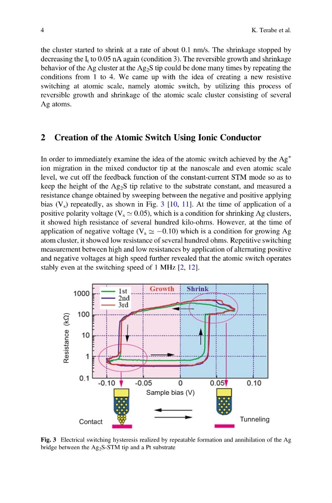
level, we cut off the feedback function of the constant-current STM mode so as to
keep the height of the Ag 2 S tip relative to the substrate constant, and measured a
resistance change obtained by sweeping between the negative and positive applying
bias (V s ) repeatedly, as shown in Fig. 3 [10, 11]. At the time of application of a
positive polarity voltage (V s ’ 0.05), which is a condition for shrinking Ag clusters,
it showed high resistance of several hundred kilo-ohms. However, at the time of
application of negative voltage (V s ’ À0.10) which is a condition for growing Ag
atom cluster, it showed low resistance of several hundred ohms. Repetitive switching
measurement between high and low resistances by application of alternating positive
and negative voltages at high speed further revealed that the atomic switch operates
stably even at the switching speed of 1 MHz [2, 12].
Resistance (kΩ)
Sample bias (V)
Tunneling
Contact
Fig. 3 Electrical switching hysteresis realized by repeatable formation and annihilation of the Ag
bridge between the Ag 2 S-STM tip and a Pt substrate
4
K. Terabe et al.
decreasing the I t to 0.05 nA again (condition 3). The reversible growth and shrinkage
behavior of the Ag cluster at the Ag 2 S tip could be done many times by repeating the
conditions from 1 to 4. We came up with the idea of creating a new resistive
switching at atomic scale, namely atomic switch, by utilizing this process of
reversible growth and shrinkage of the atomic scale cluster consisting of several
Ag atoms.
2 Creation of the Atomic Switch Using Ionic Conductor
In order to immediately examine the idea of the atomic switch achieved by the Ag
+
ion migration in the mixed conductor tip at the nanoscale and even atomic scale
level, we cut off the feedback function of the constant-current STM mode so as to
keep the height of the Ag 2 S tip relative to the substrate constant, and measured a
resistance change obtained by sweeping between the negative and positive applying
bias (V s ) repeatedly, as shown in Fig. 3 [10, 11]. At the time of application of a
positive polarity voltage (V s ’ 0.05), which is a condition for shrinking Ag clusters,
it showed high resistance of several hundred kilo-ohms. However, at the time of
application of negative voltage (V s ’ À0.10) which is a condition for growing Ag
atom cluster, it showed low resistance of several hundred ohms. Repetitive switching
measurement between high and low resistances by application of alternating positive
and negative voltages at high speed further revealed that the atomic switch operates
stably even at the switching speed of 1 MHz [2, 12].
Resistance (kΩ)
Sample bias (V)
Tunneling
Contact
Fig. 3 Electrical switching hysteresis realized by repeatable formation and annihilation of the Ag
bridge between the Ag 2 S-STM tip and a Pt substrate
4
K. Terabe et al.