

4.2 Multi-Pixel Interdigitated Photoconductive Emitters
75
(a)
(b)
(c)
(d)
150 μm
150 μm
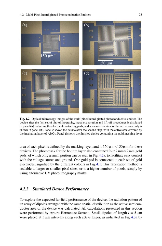
Fig. 4.2 Optical microscopy images of the multi-pixel interdigitated photoconductive emitter. The
device after the first set of photolithography, metal evaporation and lift-off procedures is displayed
in panel (a) including the electrical contacting pads, and a zoomed-in view of the active area only is
shown in panel (b). Panel c shows the device after the second step, with the active area covered by
the insulating layer of Al 2 O 3 . Panel d shows the finished device containing the gold masking layer
area of each pixel is defined by the masking layer, and is 150 µm×150 µm for these
devices. The photomask for the bottom layer also contained four 2 mm×2 mm gold
pads, of which only a small portion can be seen in Fig. 4.2a, to facilitate easy contact
with the voltage source and ground. One gold pad is connected to each set of gold
electrodes, signified by the different colours in Fig. 4.1. This fabrication method is
scalable to larger or smaller pixel sizes, or to a higher number of pixels, simply by
using alternative UV photolithography masks.
4.2.3 Simulated Device Performance
To explore the expected far-field performance of the device, the radiation pattern of
an array of dipoles arranged with the same spatial distribution as the active semiconductor area of the device was calculated. All calculations presented in this section
were performed by Arturo Hernandez Serrano. Small dipoles of length l = 5 µm
were placed at 5 µm intervals along each active finger, as indicated in Fig. 4.3a by
75
(a)
(b)
(c)
(d)
150 μm
150 μm
Fig. 4.2 Optical microscopy images of the multi-pixel interdigitated photoconductive emitter. The
device after the first set of photolithography, metal evaporation and lift-off procedures is displayed
in panel (a) including the electrical contacting pads, and a zoomed-in view of the active area only is
shown in panel (b). Panel c shows the device after the second step, with the active area covered by
the insulating layer of Al 2 O 3 . Panel d shows the finished device containing the gold masking layer
area of each pixel is defined by the masking layer, and is 150 µm×150 µm for these
devices. The photomask for the bottom layer also contained four 2 mm×2 mm gold
pads, of which only a small portion can be seen in Fig. 4.2a, to facilitate easy contact
with the voltage source and ground. One gold pad is connected to each set of gold
electrodes, signified by the different colours in Fig. 4.1. This fabrication method is
scalable to larger or smaller pixel sizes, or to a higher number of pixels, simply by
using alternative UV photolithography masks.
4.2.3 Simulated Device Performance
To explore the expected far-field performance of the device, the radiation pattern of
an array of dipoles arranged with the same spatial distribution as the active semiconductor area of the device was calculated. All calculations presented in this section
were performed by Arturo Hernandez Serrano. Small dipoles of length l = 5 µm
were placed at 5 µm intervals along each active finger, as indicated in Fig. 4.3a by