

104
5 High-Field Terahertz Time-Domain Spectroscopy …
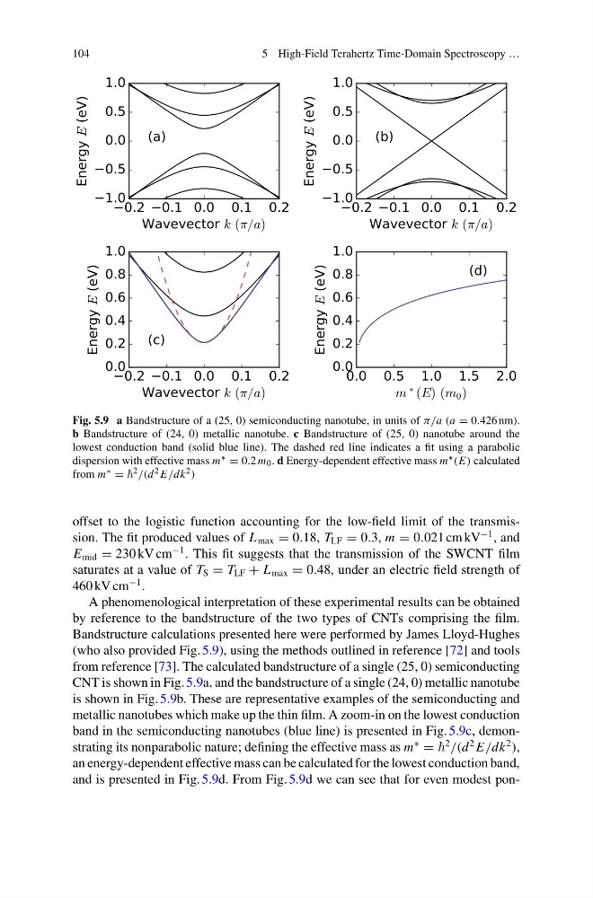
Fig. 5.9 a Bandstructure of a (25, 0) semiconducting nanotube, in units of π/a (a = 0.426 nm).
b Bandstructure of (24, 0) metallic nanotube. c Bandstructure of (25, 0) nanotube around the
lowest conduction band (solid blue line). The dashed red line indicates a fit using a parabolic
dispersion with effective mass m ∗ = 0.2 m 0 . d Energy-dependent effective mass m ∗ (E) calculated
from m ∗ = 2 /(d 2 E/dk 2 )
offset to the logistic function accounting for the low-field limit of the transmission. The fit produced values of L max = 0.18, T LF = 0.3, m = 0.021 cm kV
−1 , and
E mid = 230 kV cm
−1 . This fit suggests that the transmission of the SWCNT film
saturates at a value of T S = T LF + L max = 0.48, under an electric field strength of
460 kV cm
−1 .
A phenomenological interpretation of these experimental results can be obtained
by reference to the bandstructure of the two types of CNTs comprising the film.
Bandstructure calculations presented here were performed by James Lloyd-Hughes
(who also provided Fig. 5.9), using the methods outlined in reference [72] and tools
from reference [73]. The calculated bandstructure of a single (25, 0) semiconducting
CNT is shown in Fig. 5.9a, and the bandstructure of a single (24, 0) metallic nanotube
is shown in Fig. 5.9b. These are representative examples of the semiconducting and
metallic nanotubes which make up the thin film. A zoom-in on the lowest conduction
band in the semiconducting nanotubes (blue line) is presented in Fig. 5.9c, demonstrating its nonparabolic nature; defining the effective mass as m
∗
=
2
/(d
2 E/dk
2
),
an energy-dependent effective mass can be calculated for the lowest conduction band,
and is presented in Fig. 5.9d. From Fig. 5.9d we can see that for even modest pon-
5 High-Field Terahertz Time-Domain Spectroscopy …
Fig. 5.9 a Bandstructure of a (25, 0) semiconducting nanotube, in units of π/a (a = 0.426 nm).
b Bandstructure of (24, 0) metallic nanotube. c Bandstructure of (25, 0) nanotube around the
lowest conduction band (solid blue line). The dashed red line indicates a fit using a parabolic
dispersion with effective mass m ∗ = 0.2 m 0 . d Energy-dependent effective mass m ∗ (E) calculated
from m ∗ = 2 /(d 2 E/dk 2 )
offset to the logistic function accounting for the low-field limit of the transmission. The fit produced values of L max = 0.18, T LF = 0.3, m = 0.021 cm kV
−1 , and
E mid = 230 kV cm
−1 . This fit suggests that the transmission of the SWCNT film
saturates at a value of T S = T LF + L max = 0.48, under an electric field strength of
460 kV cm
−1 .
A phenomenological interpretation of these experimental results can be obtained
by reference to the bandstructure of the two types of CNTs comprising the film.
Bandstructure calculations presented here were performed by James Lloyd-Hughes
(who also provided Fig. 5.9), using the methods outlined in reference [72] and tools
from reference [73]. The calculated bandstructure of a single (25, 0) semiconducting
CNT is shown in Fig. 5.9a, and the bandstructure of a single (24, 0) metallic nanotube
is shown in Fig. 5.9b. These are representative examples of the semiconducting and
metallic nanotubes which make up the thin film. A zoom-in on the lowest conduction
band in the semiconducting nanotubes (blue line) is presented in Fig. 5.9c, demonstrating its nonparabolic nature; defining the effective mass as m
∗
=
2
/(d
2 E/dk
2
),
an energy-dependent effective mass can be calculated for the lowest conduction band,
and is presented in Fig. 5.9d. From Fig. 5.9d we can see that for even modest pon-