

2.4 Genealogy of Memristor Devices
63
The above examples make clear that:
• every ideal memristor spawns an infinite family of equivalent ideal generic
memristor siblings;
• two ideal generic memristors whose state variables are related by a one-toone differentiable transformation have identical signatures and properties (e.g.,
pinched hysteresis loops). This property is named memristor state variable
transform property.
For example, the HP memristor [28] is a sibling of an ideal memristor and this is
true also for memristor devices described by a mathematical models obtained from
the HP memristor and based on window functions introduced to bound the state
variables domain [29–32].
2.4.2.1 The HP Memristor
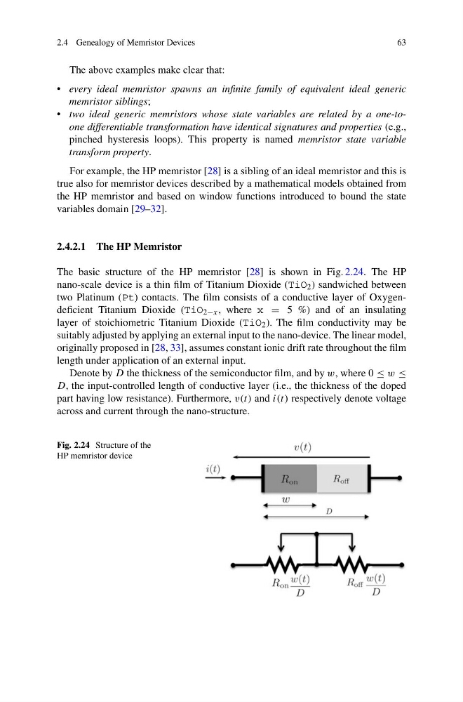
The basic structure of the HP memristor [28] is shown in Fig. 2.24. The HP
nano-scale device is a thin film of Titanium Dioxide (TiO 2 ) sandwiched between
two Platinum (Pt) contacts. The film consists of a conductive layer of Oxygendeficient Titanium Dioxide (TiO 2−x , where x = 5 %) and of an insulating
layer of stoichiometric Titanium Dioxide (TiO 2 ). The film conductivity may be
suitably adjusted by applying an external input to the nano-device. The linear model,
originally proposed in [28, 33], assumes constant ionic drift rate throughout the film
length under application of an external input.
Denote by D the thickness of the semiconductor film, and by w, where 0 ≤ w ≤
D, the input-controlled length of conductive layer (i.e., the thickness of the doped
part having low resistance). Furthermore, v(t) and i(t) respectively denote voltage
across and current through the nano-structure.
Fig. 2.24 Structure of the
HP memristor device
63
The above examples make clear that:
• every ideal memristor spawns an infinite family of equivalent ideal generic
memristor siblings;
• two ideal generic memristors whose state variables are related by a one-toone differentiable transformation have identical signatures and properties (e.g.,
pinched hysteresis loops). This property is named memristor state variable
transform property.
For example, the HP memristor [28] is a sibling of an ideal memristor and this is
true also for memristor devices described by a mathematical models obtained from
the HP memristor and based on window functions introduced to bound the state
variables domain [29–32].
2.4.2.1 The HP Memristor
The basic structure of the HP memristor [28] is shown in Fig. 2.24. The HP
nano-scale device is a thin film of Titanium Dioxide (TiO 2 ) sandwiched between
two Platinum (Pt) contacts. The film consists of a conductive layer of Oxygendeficient Titanium Dioxide (TiO 2−x , where x = 5 %) and of an insulating
layer of stoichiometric Titanium Dioxide (TiO 2 ). The film conductivity may be
suitably adjusted by applying an external input to the nano-device. The linear model,
originally proposed in [28, 33], assumes constant ionic drift rate throughout the film
length under application of an external input.
Denote by D the thickness of the semiconductor film, and by w, where 0 ≤ w ≤
D, the input-controlled length of conductive layer (i.e., the thickness of the doped
part having low resistance). Furthermore, v(t) and i(t) respectively denote voltage
across and current through the nano-structure.
Fig. 2.24 Structure of the
HP memristor device